

Translate this page into:
Method to control the optical properties: Band gap energy of mixed halide Organolead perovskites
⁎Corresponding author. fabian.ezema@unn.edu.ng (Fabian I. Ezema)
-
Received: ,
Accepted: ,
This article was originally published by Elsevier and was migrated to Scientific Scholar after the change of Publisher.
Peer review under responsibility of King Saud University.
Abstract
Abstract
In this work, we studied the effect of varying the volume of mixed halide perovskites on the structural, morphological and optical properties of deposited thin films. A two-step process of spin coating and dipping technique was employed so as to enhance deposition of the films. The samples were subjected to heat treatment after each deposition cycle in order to increase the crystalinity and grain size of the films. The band gap, refractive index, dielectric constant and optical conductivity of the mixed halide perovskites were calculated. The single term Wemple DiDomenico oscillator formulae were applied in determining the expression of the parameter n below the optical band gap in relation to the energy.
A significant observation in this study was that the band gap of mixed halide perovskites was extremely lowered compared to the high band energy of its halide perovskite, which reveals the band gap alteration effect of mixed halide perovskites. The refractive index and dielectric constant of the halide and mixed halide perovkites showed results in the wavelength range of 300–600 nm, which is significant for photovoltaic materials.
Keywords
Thin film
Mixed halide perovskites
Band gap
Refractive index
Dielectric constant

1 Introduction
Photovoltaic (PV) cells are devices that convert solar radiation directly to electricity. Silicon based solar cell possess advantages such as hardness and high temperature stability, which have made them favorable for photovoltaic applications. Promising technologies combines both low cost and ease of fabrication for an improved energy output, thereby replacing silicon based devices. Thin film solar cell such as CuInGaSe2 (Repins et al. 2008), organic solar cell (Service, 2011) and dye sensitized solar cells DSSC (O’Regan and Grätzel, 1991) are cheaper and are presently used as substitutes for silicon based solar cells (Sheikh, et al., 2015). Though these substitutes are low-cost, but have a challenge of low efficiency and stability. The advent of organometallic halide perovskites offers attractive prospects (Green et al. 2014; Hodes & Cahen, 2014; Heo et al. 2015). Recently, the perovskite sensitizer ABX3 (A = CH3NH3, B = Pb, Sn, and X = Cl, Br, I) attracted great attention as a result of its excellent light-harvesting characteristics (Kim et al., 2012; Liu et al., 2013; Wojciechowski et al., 2012; Im et al., 2011).
Perovskites are made up of economical and earth abundant materials. In addition, it generates charges freely in the bulk material after light absorption that enables low energy-loss charge generation and collection (Stranks et al., 2013; Wehrenfennig et al., 2014). The perovskite films are usually polycrystalline in nature, with large surface area and grain boundaries (GBs). Therefore, it is important to exploit the surface/interfaces and GBs in the perovskite films that affect the carrier functionality in the heterojunction. Over the years various techniques have been developed to achieve subtle control over the film property so as to promote charge generation, transportation, and collection in the solar cell. Specifically, the iodide and bromide versions of CH3NH3PbX3 have led a revolution performance in thin film solar cells (Kim et al., 2012). The use of mesoporous metal oxides, such as Titania (Kojima et al., 2012) and Alumina (Snaith et al., 2013) was first reported in the fabrication of perovskites cells for photovoltaic applications whose porosity permits the formation of CH3NH3PbX3 perovskite nano particulate material, i.e., the confinement of the array extending in three dimensions. The first perovskite sensitized solar cells was studied, utilizing CH3NH3PbI3 and CH3NH3PbBr3 as light absorbers on TiO2 mesoporous layers with halide electrolytes (Kojima et al., 2009). A noteworthy efficiency of 3.81% was obtained from CH3NH3PbI3 with photocurrent recorded from a wavelength of ∼800 nm. An impressive photo voltage of 0.96 V was obtained from CH3NH3PbBr3, which was attributed to the deep bromide redox couple used in such solar cells. CH3NH3PbI3 absorber in an iodide/triiodide redox couple achieved an efficiency of 3.5% (Kim et al., 2012). Snaith et al., 2013 on the other hand utilized a mixed halide system – CH3NH3PbI3-xClx on both TiO2 and Al2O3 mesoporous layers and obtained a very high efficiency (PCE = 10.9%, JSC = 17.8 mA cm−2, VOC = 0.98 V and FF = 0.63) for the mesoporous Al2O3 devices. An approach by Kumar et al., 2013 employed electrodeposited ZnO on rigid FTO and flexible ITO on which CH3NH3PbI3 was spin coated, thereafter they used another approach where ZnO nanoparticles were spin coated from a solution of a butanol/chloroform mixture, of which the authors argue that the lack of a constricting mesoporous layer allows for unconstrained CH3NH3PbI3 perovskite crystal growth thereby yielding an impressive efficiency of 15.7% on FTO and 10.2% on flexible ITO substrates. There are only few reports on perovskites with NiO (Etgar et al., 2012). Also, Perovskite has been studied for used in heterojunction devices with 2D crystals (graphene) which was reported to produce photo-responsitivity of ∼950 A/W and a high on/off ∼106 ratio behavior transistor (Cheng et al., 2016).
In this study, we employed dipping technique to deposit the perovskites on glass substrates. We determined the effect of mixed halide perovskites on the structural, morphological and optical properties for solar cell application. To the best of our knowledge it is the first time that the volumetric combination of mixed halide perovskite is being studied though Atourki et al., 2016 carried out a study on mixed halide perovskites but their research was limited to MAPbI3 and MAPBr3 mixed halide perovskites. The study by Green et al. (2014), is one of the few research where formamidinium lead iodide (FAPbI3) is used to obtain, mixed halide perovskites. Although, Longfei et al., 2016 synthesized and studied cesium lead halide perovskites and its mixed halide perovskites nanosheets for photodetector application, only a few studies have been carried out on mixed methylammonium lead halide perovskites. The objective of this study is to determine the effect of the combination of three mixed halide perovskites (MAPbI3, MAPBr3, MAPbCl3) on the optical properties of the films. The halide perovskites: MAPbCl and MAPbBr were combined at various volumetric ratios (0.6 ml – 1.4 ml) with a fixed volume of MAPbI (2 ml) in this study. Our study will help understand the role and impact of these methyl ammonium based perovskites on optical properties of the films.
2 Experimental details
The methyl ammonium based perovskites were synthesized using Methylamine (MA) 35 ml and hydroiodic acid (HI) 40 ml (for MAI), hydrobromic acid (HBr) for (MABr) or hydrochloric acid (HCl) for MACl. 35 ml of MA with 40 ml of one of these acids (HI, HBr, and HCl) respectively were poured into a round bottom flask stirred at 0 °C for 2hrs. After which the solution was heated in a beaker at 80 °C until the solution has completely evaporated, leaving a white precipitate. The precipitate was left to cool, after which it was washed with acetone for three consecutive times, filtered and dried in an oven at 60 °C. PbI, PbCl and PbBr were synthesized using lead nitrate (PbNO3) with each of these salts: KI, KCl and KBr. The resulting solutions were stirred at 80 °C for 30 min, after which the precipitate was cooled, filtered and dried in the oven.
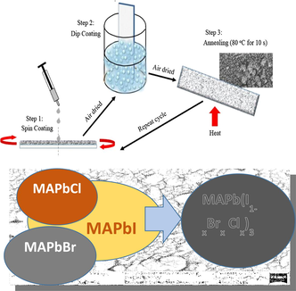
Equimolar MAI, MABr, MACl and PbI, PbBr, PbCl respectively was dissolved in γ- butylactone and stirred at 80 °C for 2 h for proper mixture. 2 ml of MAPbI was added to varying volume (0.6, 0.8. 1.0, 1.2, 1.4 ml) of MACl and MABr, then 2 ml each of the three halide perovskite was mixed together. The perovskite solution mixture was spin coated on the glass substrates at a revolution of 2000 rpm so as to enhance the adherence of the perovskite on the substrate, then the substrate was air dried for 10 s, dipped into perovskite solution for 20 s, air dried again then annealed on a hot plate at 80 °C for 10 s. These processes were repeated until a good film thickness was obtained. The schematic deposition procedure for halide and mixed halide perovskite is shown in Fig. 1.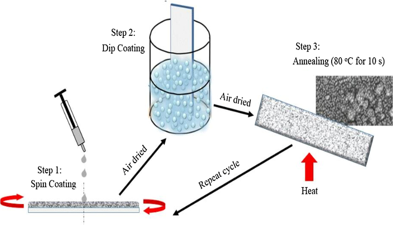
A schematic representation steps to the development of the halide and mixed halides perovskite thin films for solar cell fabrication.
Chemical equation of the synthesis reactions:
The prepared films were characterized for their structural properties using an automatic powder diffractometer X’pert Pro with a theta-theta goniometer, an ultrafast semiconductor detector Pixcel and CuKα radiation (λ ∼ = 0.154 nm), morphological properties using Carl Zeiss Ma-10 field emission electron microscope operating at 20 keV with an accelerating voltage of 5.0 kV and for the optical studies, the Absorbance data of the films was obtained using UV-1800 Schimadzu spectrophotometer with wavelength between 400 and 1000 nm.
3 Results and discussion
3.1 Structural studies
Fig. 2 shows the X-ray diffraction patterns of halides and mixed halide perovskites of MAPbI3 with different volumes of MAPbBr3 and MAPbCl3. As the bromide content was increased, we observed different diffraction profiles shifting toward higher angles. This may be due to the limited substitution of the iodine atom resulting in decrease in the lattice space between each atom. The pure MAPbI3 sample presents a small diffraction peak matching at 11.87° and 13.26° and can be attributed to the crystal planes (0 0 1) and (0 0 4) with an hexagonal structure. The presence of PbI diffraction peaks with small intensity was observed. This peak has been often identified in thin film X-ray diffraction, and may be an indicator of a minor decomposition of the samples (Baikie et al., 2013). We observed that addition of PbBr slightly increased the diffraction peaks as seen in Fig. 2 (a). The pure MAPbCl sample presented no prominent diffraction peak compared to other samples MAPbI3 + 1.0 ml MAPbBr3 and MAPbI3 + 1.4 ml MAPbBr3 which show relatively strong peak intensity at 13.26°, 39.54°, 65.46°, and 43.20°, which correspond to the planes of (004∗), (003∗∗) and (004∗∗). Sample MAPbI3 + 0.6 ml MAPbBr3 gave highest intensity peaks at 13.26° and 30.10° corresponding to the plane (004∗) and (0 0 2), while sample MAPbI3 + 0.8 ml MAPBr3 and MAPbI3 + 1.2 ml MAPBr3 showed only one peak at 13.26° corresponding to the plane (004∗). However, the presence of the PbI phase may be due to the solution interaction of MAPbBr3/MAPbI3 that leaves a small amount of MAPbI3 unreacted (Atourki et al., 2016).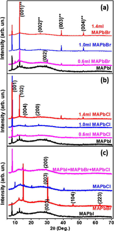
X-ray diffraction profiles of methyl ammonium based perovskites, comprising of MAPbI3 with different amount of (a) MAPbBr3 and (b) MAPbCl3. (c) Diffractograms of individual perovskites and a combination of the three components.
Furthermore, Fig. 2 (b) shows the X-ray diffraction patterns of MAPbI3 with varying volume of MAPbCl3. As the volume of the MAPbCl3 content increased, the intensity peaks also increased. It was found that all samples patterns are in good accordance with the hexagonal structure and peaks at 7.70° and 13.47° can be attributed to the crystal planes (0 0 1) and (1 0 2) respectively (Huangfu et al., 2015). The MAPbI3 + 1.4 ml MAPbCl3 sample also showed various smaller peaks at different angles, located at 39.44° and 53.24°. The MAPbI3 + MAPbBr3 + MAPbCl3 mixed halide perovskite sample showed very few peaks as compared to the other perovskites as shown in Fig. 2(c).
The intensity of the diffraction peaks increases with the volumes of MAPbBr3 and MAPbCl3 used to prepare them. The engineered crystalline structures of the mixed halide perovskites tend to grow into amorphous form as the complexity of the composite perovskites is increased.
3.2 Morphological studies
The MAPbI3 micrograph in Fig. 3 showed a bubble-like morphology while MAPbBr3 and MAPbCl3 showed trapezoid-like grains. The mixed perovskites methylammonium lead iodide (MAPbI3) and methythylammonium lead bromide (MAPbBr3) at various volumes form large central grains which were observed to be disjointed as the volume of the halides perovskite in the mixture was increased. A similar effect was observed for the volumetric methylammonium lead chloride (MAPbCl3) samples, however, the surface of the films were cracked at lower volume mixture and more bubble-like grains were observed. A similar defect was reported by Park, et al., (2015) for MAPbCl3 perovkites. We may attribute the central grain morphology obtained for MAPbBr3 mixed perovskite to the precursor used in the synthesis process. This is also in agreement the reports by Cacovich et al., 2015 and Vrućinić et al., 2015. In the three halide perovskites: MAPbI3: MAPbBr3: MAPbCl3 of the same volumetic proportion, we observed a finer morphology compared to the morphologies of other samples which may be as a resulting effect of the perovskites combination.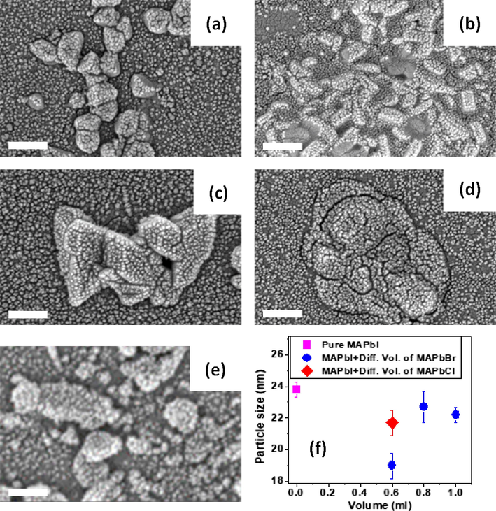
SEM micrographs of the halide and mixed halide perovskites. The samples comprised of MAPbI3 and (a) 0.6 ml MAPbCl3, (b) 0.6 ml MAPbBr3, (c) 0.8 ml MAPbBr3 (d) 1.0 ml MAPbBr3 and (e) Pure MAPbI3. The scale bar in the micrographs represents 200 nm. (f) The particles size of pure MAPbI3 and the mixed halide perovskites as a function of the volume of the MABr and MACl used to prepare them. The error bar is the standard deviation of the particle size estimated from over 200 particles in the micrograph.
It was evident that mixing the perovskite definitely changes the surface morphologies of the perovskite films. It has also been reported that the presence of bromide increases the roughness of the surface morphology of perovkites (Ilmaz et al., 2016; Atourki et al., 2016). The increased grain size and crystals observed in the perovskite with varying volumetric ratio of methylammonium lead bromide was favorable for homogeneous phase retention of the mixed halide perovskite during the photoexcitation (Hu et al., 2016). Perovskites with relatively large grain boundaries are required for possible recombination paths and for improving carrier transport and lifetime (Fang et al., 2016; Song et al., 2015).
3.3 Optical studies
Perovskites based solar cells performance depends on the charge carriers as well as light absorbing property (Lee et al., 2012; Dualeh et al., 2013). It was observed that increasing the volumetric ratio of methylammomium lead bromide introduced to a fixed volume of MAPbI3, increases the absorption edge of the hybrid perovskite as seen in Fig. 4. A similar result was reported by (Aharon et al., 2014). This shift in the absorption edge was observed in all samples of the mixed hybrid perovskite. In the samples of varying volume of methylammonium lead chloride we observed an abnormal change in the absorption edge where it increased greatly compared to its pure samples, and the samples containing 1.2 and 1.4 ml of methylammmonium lead chloride the absorption edge was indifferent from their parent samples MAPbI3 & MAPbCl3.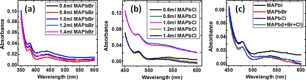
Variation of the absorbance with wavelength for mixed halide perovskites comprising of MAPbI3 with different amount of (a) MAPbBr3 and (b) MaPbCl3. (c) Absorbance of individual halide perovskites and a combination of the three components.
This result may be attributed to the variation in the substitution of I- atoms by MAPbI3 atom (Comin et al., 2015; Jiang et al., 2015). At lower Br content, the mixed halide perovskites MAPb(I1−xBrx)3 exhibit an extended absorption over the visible light spectrum, which is favorable for light harvesting. The higher the Br content, the absorption onset gradually shifts to the higher photon energy, i.e., to shorter wavelength of light (Jong et al., 2016; Beal et al., 2016).
The absorption coefficient is the parameter which determines how far into a material light of a particular wavelength can penetrate before it is absorbed, it was obtained (Pankove, 1971):
The type of transition between the valence and conduction band of the perovskite sample is described by the plot of absorption coefficient, ‘α’ against the photon energy, ‘hν’ presented in Fig. 5. The thin film material showed a low absorption coefficient, which means that light is poorly absorbed. Semiconductor materials have a sharp edge in their absorption coefficient, because light energy below the band gap does not have sufficient energy to excite an electron into the conduction band from the valence band, therefore this light is not absorbed.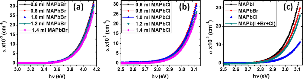
Plots of absorption coefficients versus photon energy, hν for mixed halide perovskites comprising of MAPbI3 with different amount of (a) MAPbBr3, (b) MaPbCl3 and (c) a combination of the three halide perovskites.
In Fig. 6 and the plots of band gap versus photon energy shown in the supplementary material Fig. S1, we present the values of the band gap of the halide and mixed halide perovskites.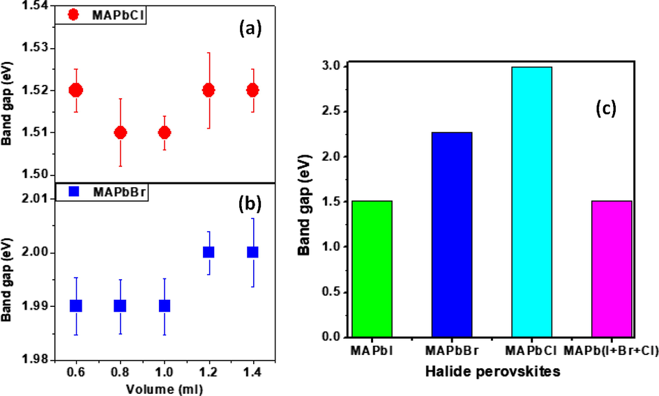
Variation of band gap energy with volumes of individual halide perovskites used to form the mixed halide perovskites. Each sample comprised of MAPbI3 with different volumes of (a) MAPbCl3 and (b) MAPbBr3. (c) Histogram of band gap energy of individual halide perovskites and a combination of the three components.
Fig. 7 shows the refractive index of the perovskite samples, only a slight difference was observed in their values but samples containing varying volumetric ratio of MAPbCl3 we observed an arm which extended further towards the visible region while the reverse was seen in samples with varying volumetric ratio of MAPbBr3.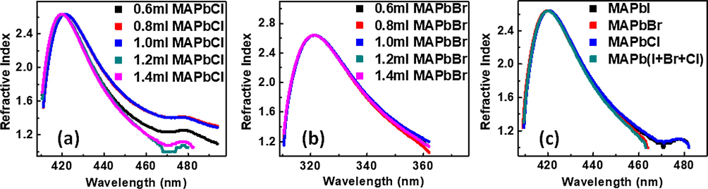
Plots of refractive index, n versus wavelength, λ for mixed halide perovskites comprising of MAPbI3 with different amount of (a) MAPbCl3, (b) MAPbBr3 (c) combination of the three halide perovskites.
The average value of the refractive index of the films was 2.73.The extinction coefficient plots and discussion are seen the supplementary material. The plots of the extinction coefficient versus wavelength are shown in the supplementary material Fig. S2.
The optical parameters n and the k were determined from Eqs. (2) and (3) (Yildirim et al., 2017; Yildirim et al., 2016):
In Fig. 8 the values of the real and imaginary parts of the dielectric constant are plotted and directly related to the refractive indices using these equations
;
. The difference in the values obtained for the various samples may be related to deposition technique used, which produce layers of non-uniform thickness.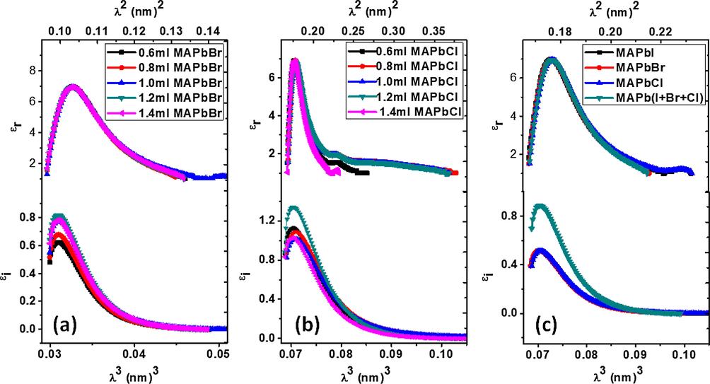
Plots of Real,
and imaginary,
dielectric constants versus wavelengths, λ2,λ 3 for mixed halide perovskites comprising of MAPbI3 with different amount of (a) MAPbBr3, (b) MaPbCl3 (c) combination of the three halide perovskites.
Also, samples with similar chemical composition fabricated with similar procedures can produce different grain size distributions which affect their values due to the different levels of scattering (Egger, 2015). A higher dielectric constant indicates a greater ability to screen charge which could arise from electronic or ionic contributions, as well as the methylammonium molecular dipoles in the lattice (Frost et al., 2014). All samples possess high dielectric value but MAPbI3, MAPbBr3, MAPbCl3 perovskites in their uncombined state have lower imaginary dielectric value. Also, high dielectric constant reduces the spatial extent and the potential barrier of a charged defect, thereby lowering the tendency to scatter free carriers. Recombination models to categorize the underlying electronic structure parameters of MAPbX3 with high experimentally observed lifetime and mobility include: dielectric constant, effective mass, band bonding character, and band dispersion. The single term Wemple DiDomenico oscillator plots and discussion is found in the supplementary material.
From the Drude free electron model the dependence of ‘
’ and ‘
’on the wavelength can be written by the following relations (Saadeddin et al., 2007):
The optical conductivity was estimated using (Abd El-Raheem, 2007):
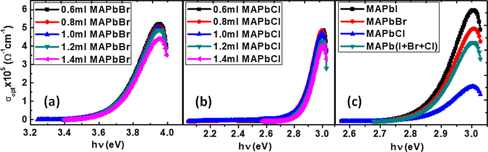
Plots of Optical conductivity versus photon energy, hν for mixed halide perovskites comprising of MAPbI3 with different amount of (a) MAPbBr3, (b) MaPbCl3 (c) combination of the three halide perovskites.
Another trend that was observed from the plots was a decrease in the optical conductivity as the volumetric ratio of MAPbBr3 and MAPbCl3 increased, and also there was a shift in the photon energy point where the maximum optical conductivity occurred in MAPbBr3 mixed halide perovskites, this could be attributed to the influence of MAPbBr3 on the mixed halide perovskite. The average value of the optical conductivity of the films was 6 × 10⁵ S/m.
4 Conclusion
In this study, we have successfully studied the effect of mixed halide perovskites on the optical, morphological and structural properties of halide perovskites. We discovered that mixed halide perovskites possessed a unique property for band gap engineering, of which the band gap was in the range of 1.51–3.0 eV. MAPbCl3 perovskite gave a very wide band gap which was drastically reduced by it combination with MAPbI3 thereby increasing its range of application. The structural and morphological properties of the film reveal an enhancement of the grain size and crystals of the mixed halide perovskites. An average value of 2.73 was obtained for the refractive index and the dielectric constants of the mixed halide perovskites were only slightly altered. Optical conductivity gave an average value of 6 × 10⁵ S/m for all perovskite samples but MAPbI3 gave the highest conductivity of 8 × 10⁵ S/m. Our findings showed the following results: the optical conductivity of mixed halide perovskite decreases with increase in volume of MAPbBr3 or MAPBCl3, the band gap of the three combined perovskites was similar to that of MAPbI3, the refractive index was only slightly altered, all samples of the mixed halide perovskites have a high dielectric constant which reduces the spatial extent and potential barrier of a charged defect, thereby lowering the tendency to scatter free carriers.
Acknowledgements
We graciously acknowledge the grant for this project by TETFUND under contract number TETF/DESS/UNN/NSUKKA/STI/VOL.I/B4.33. We thank the US Army Research Laboratory–Broad Agency Announcement (BAA) for the financial support given to this research (under Contract number W911NF-12-1-0588). Also we thank Engr. Emeka Okwuosa for generous sponsorship of April 2014 and July, 2016 conference/workshops on applications of nanotechnology to energy, health &.Environment conference.
References
- Optical properties of GeSeTl thin films. J. Phys.: Condens. Matter. 2007;19(216209):1-7.
- [Google Scholar]
- Hybrid lead halide iodide and lead halide bromide in efficient hole conductor free perovskite solar cell. J. Phys. Chem. C 2014:17160-17165.
- [Google Scholar]
- Materials, role of the chemical substitution on the structural and luminescenceproperties of the mixed halide perovskite thin MAPbI3 – xBrx (0 ≤ x ≤ 1) films. Appl. Surf. Sci.. 2016;371:112-117.
- [Google Scholar]
- Synthesis and crystal chemistry of the hybrid perovskite (CH3NH3) PbI3 for solid-state sensitised solar cell applications. J. Mater. Chem.. 2013;A1:5628-5641.
- [Google Scholar]
- Determination of the optical parameters of a-Si: H thin films deposited by hot wire–chemical vapour deposition technique using transmission spectrum only, Pramana. J. Phys.. 2011;76:519-531.
- [Google Scholar]
- Cesium Lead Halide Perovskites with Improved Stability for Tandem Solar Cells. J. Phys. Chem. Lett.. 2016;7:746-751.
- [Google Scholar]
- Nanoscale investigation of organic – inorganic halide perovskites. J. Phys.: Conf. Series. 2015;644:012024.
- [Google Scholar]
- Van der Waals heterojunction devices based on organohalide perovskites and two-dimensional materials. Nano Letters. 2016;16(1):367-373.
- [Google Scholar]
- Structural, optical, and electronic studies of wide-bandgap lead halide perovskites. J. Mater. Chem. C. 2015;3:8839-8843.
- [Google Scholar]
- Impedance spectroscopic analysis of lead iodide perovskite-sensitized solid-state solar cells. Am. Chem. Soc. Nano. 2013;8:362-373.
- [Google Scholar]
- Perovskite Solar Cells: Do We Know What We Do Not Know? Journal of Physical Chemistry Letters. 2015;6:279-282.
- [Google Scholar]
- Mesoscopic CH3NH3PbI3/TiO2 heterojunction solar cells. J. Am. Chem. Soc.. 2012;134:17396-17399.
- [Google Scholar]
- Ultrahigh sensitivity of methylammonium lead tribromide perovskite single crystals to environmental gases. Advancement of Science. 2016;2(e1600534):1-9.
- [Google Scholar]
- Atomistic origins of high performance in hybrid halide perovskite solar cells. Nano Lett.. 2014;14:2584-2590.
- [Google Scholar]
- Planar CH3NH3PbI3 perovskite solar cells with constant 17.2% average power conversion efficiency irrespective of the scan rate. Adv. Mater.. 2015;27(22):3424-3430.
- [Google Scholar]
- Wide Bandgap Organo-lead Trihalide Perovskites for Solar Cells. Lincoln: University of Nebraska; 2016.
- Copper iodide as inorganic hole conductor for perovskite solar cells with different thickness of mesoporous layer and hole transport layer. Appl. Surf. Sci. 2015
- [CrossRef] [Google Scholar]
- Ilmaz, O., 2016. Optical and structural characterization of mixed halide perovskite thin films fabricated by thermal co-evaporation a thesis submitted to the graduate school of natural and applied sciences of middle-east technical University.
- 6.5% efficient perovskite quantum-dot-sensitized solar cell. Nanoscale. 2011;3:4088-4093.
- [Google Scholar]
- Enhancing the performance of planar organo-lead halide perovskite solar cells by using a mixed halide source. J. Mater. Chem. A. 2015;3:963-967.
- [Google Scholar]
- Influence of halide composition on the structural, electronic and optical properties of mixed CH3NH3Pb(I1−xBrx)3 perovskites with virtual crystal approximation method. Phys. Rev. B. 2016;94:125139.
- [Google Scholar]
- Lead iodide perovskite sensitized all solid-state submicrons thin film msesoscopic solar cell with efficiency exceeding 9%. Nat. Sci. Report. 2012;2:591.
- [Google Scholar]
- Highly luminescent lead bromide perovskite nanoparticles synthesized with porous alumina media. Chem. Lett.. 2012;41:397.
- [Google Scholar]
- Organometal halide perovskites as visible-light sensitizers for photovoltaic cells. J. Am. Chem. Soc.. 2009;131:6050-6051.
- [Google Scholar]
- Flexible, low-temperature, solution processed ZnO-based perovskite solid state solar cells. Chem. Commun.. 2013;49:1089-11091.
- [Google Scholar]
- Efficient hybrid solar cells based on meso-super structured organometal halide perovskite. Science. 2012;338:643-647.
- [Google Scholar]
- Efficient planar heterojunction perovskite solar cells by vapour deposition. Nature. 2013;501:395-398.
- [Google Scholar]
- Generalized colloidal synthesis of high-quality, two-dimensional cesium lead halide perovskite nanosheets and their applications in photodetectors. Nanoscale. 2016;8:13589-13596.
- [Google Scholar]
- Conduction in non-crystalline systems V conductivity, optical absorption and photoconductivity in amorphous semiconductors. Philos. Mag.. 1970;22:0903-0922.
- [Google Scholar]
- A low-cost, high-efficiency solar cell based on dye-sensitized colloidal TiO2 films. Nature. 1991;353:737-740.
- [Google Scholar]
- Optical processes in semiconductors (1st ed.). New Jersy: Prentice Hall; 1971. pp 34.
- Chemical engineering of methylammonium lead iodide/bromide perovskites: tuning of optoelectronic properties and photovoltaic performance. J. Mater. Chem. A. 2015;3:21760-21771.
- [Google Scholar]
- 19·9% Efficient ZnO/CdS/CuInGaSe2 solar cell with 81·2% fill factor. Prog. Photovol. : Res. Appl.. 2008;16(3):235-239.
- [Google Scholar]
- Synthesis and characterization of single- and co-doped SnO2 thin films for optoelectronic applications. Appl. Surf. Sci.. 2007;253:5240-5249.
- [Google Scholar]
- Atmospheric effects on the photovoltaic performance of hybrid perovskite solar cells. Sol. Energy Mater. Sol. Cells. 2015;137:6-14.
- [Google Scholar]
- Perovskites: the emergence of a new era for low-cost, high-efficiency solar cells. Journal of Physical Chemistry Letters. 2013;4:3623-3630.
- [Google Scholar]
- Perovskite solar cells: film formation and properties. J. Mater. Chem. A 2015:9032-9050.
- [Google Scholar]
- Electron-hole diffusion lengths exceeding 1 micrometer in an organometal trihalide perovskite absorber. Science. 2013;342:341-344.
- [Google Scholar]
- Local versus long-range diffusion effects of photoexcited states on radiative recombination in organic-inorganic lead halide perovskites advanced. Science. 2015;2(9):1500136.
- [Google Scholar]
- High charge carrier mobilities and lifetimes in organolead trihalide perovskites. Adv. Mater.. 2014;26:1584-1589.
- [Google Scholar]
- Sub-150°C processed meso-superstructured perovskite solar cells with enhanced efficiency. Energy Environ. Sci.. 2012;7:1142-1147.
- [Google Scholar]
- Refractive index and optical absorption properties of the complexes of a cyclobutane containing thiazolylhydrazone ligand. Opt. Mater.. 2005;27:1363-1368.
- [Google Scholar]
- Investigation of structural, optical and dielectrical properties of Cu2WS4 thin film. J. Mater. Sci.: Mater. Electron.. 2017;28(9):6712-6721.
- [Google Scholar]
- Optical characterization of Cu2ZnSnSe4-xSx nanocrystals thin film. J. Alloy Compd.. 2016;666:144-152.
- [Google Scholar]
Appendix A
Supplementary material
Supplementary data associated with this article can be found, in the online version, at https://doi.org/10.1016/j.arabjc.2017.09.002.
Appendix A
Supplementary material
Supplementary data 1
Supplementary data 1