

Translate this page into:
C60 adsorption on defective Si (1 0 0) surface having one missed dimer from atomic simulations at electrical level
⁎Corresponding author. zhanglin@imp.neu.edu.cn (Lin Zhang)
-
Received: ,
Accepted: ,
This article was originally published by Elsevier and was migrated to Scientific Scholar after the change of Publisher.
Peer review under responsibility of King Saud University.
Abstract
The adsorption geometry and electronic information of C60 onto reconstructed Si (1 0 0) surface having two types of missed dimers were investigated from self-consistent charge density functional tight-binding (SCC-DFTB) simulations. The C60 molecular orientation being relative to the defective Si surface, bonding form, and the number and distribution of dimers in the silicon surface, greatly affect the packing configurations in the C60/Si (1 0 0) systems. Charge-difference density and Mulliken populations analysis indicated that C60 was chemically bound to the silicon substrate by C-Si covalent bonds and the bond energy of short C—Si covalent bonds is higher than others. The different adsorption configurations of C60/Si systems have different chemical potentials, implying their various applications in the redox reactivity.
Keywords
Atomic simulations
DFTB
Surface defect
C60
Si

1 Introduction
During recent decades, molecular electronics proposed in 1970s have been recognized as one of the objectives in applications of nano-technology and developing new devices to replace solid electronic components at the molecular level. Nanotechnology has been recognized as a revolutionary field of science and technology (Xi et al., 2022; Liu et al., 2022a; Liu et al., 2022b; Liu et al., 2022c; Liu et al., 2022d; Qu et al., 2022; Wang et al., 2019). For example, graphene and its related research are reported in detail in articles (Yoosefian et al., 2022; Yoosefian et al., 2020; Zaghmarzi et al., 2017; Yoosefian et al., 2018; Cao et al., 2020). Nanoscale manipulation of organic molecules on crystal surfaces by using scanning tunneling microscopy (STM) (Gimzewski et al., 1999) and atomic force microscopy (AFM) (Trache et al., 2008; Hobbs et al., 2005) has been used to achieve the nanostructures on atoms’ or molecules’ packing. For example, the adsorption of C60 molecules on Si(1 0 0) surfaces by STM (Dong et al., 1995; Demuth et al., 1987) and the morphology of vacuum-deposited thin films of C60 on Si(1 0 0) and InP(1 0 0) semiconductor surfaces were investigated by AFM (Basiuk et al., 2003). Various reconstructed Si surfaces play a key role in controlling cycloaddition reactions through utilizing dangling bonds on the surface and unsaturated organic precursors to form ordered organic thin films (Yoshinobu, 2004). Typical adsorptions on Si(1 0 0), including trimethylamine, ammonia, water, boron fluoride (BF3), ethylene and vinyl bromide have been investigated experimentally (Luy et al., 2021; Meng et al., 2017; Sundberg et al., 2014). It is well known that the high density of π electrons of C60 molecule can serve as a potential replacement for small organic molecules. As a prototype nano-fullerene-molecule, C60 presents interesting characteristics including spherical shape with high symmetry and easily handling, and it is expected to provide usefully electronic and optical functionalities. In fact, C60 adsorbed on the perfect Si(1 0 0) surface have received great attention in connection with the development of new molecular devices combined with current semiconductor technology (Lee et al., 2007; Senftleben et al., 2008; Godwin et al., 2003). One of potential applications is a spin-based solid-state quantum computer. It has been proposed that such a device could be constructed from doped endohedral fullerenes as the carrier of the qubit, coupling with adjacent endohedral atoms through hyperfine interactions. The fullerenes positioned on the Si surface provide gates to read and input the quantum states and control the coupling (Harneit et al., 2002; Meyer et al., 2004) as described in the reference (Chen et al., 2011). In an earlier work, the immobilisation of C60 derivatives on various semiconducting surfaces has been concerned (Cattaruzza et al., 2008; Bonifazi et al., 2002). Specifically, a series of fullerene-derived carboxylic acids can be easily adsorbed on (n- and p-type) GaAs and ZnO crystals, revealing a strong influence of the electron-accepting fullerene moieties on the superficial properties (work function and band bending) of the semiconductor as a consequence of the interaction between the frontier orbitals of the carbon spheres. In particular, the self-assembly of C60 molecules on flat Si(1 0 0) surfaces via direct tethering of the carbon sphere to the surface as shown by electrochemical and fast atom bombardment mass spectrometry measurements. All fullerene-containing materials were found to be very stable in both acidic aqueous and polar non-aqueous solvents (Lee et al., 2008). However, due to the manufacturing processes or oxidization from various small molecules or oxides, the Si surface usually has defects. Si/C60 multilayers composed of semiconductors Si and C60 exhibit incomplete photonic bandgap properties in the visible wavelength band, and can be used to prepare some novel photonic devices, which has far-reaching implications for the application of photonic crystals as substrate materials for small planar antennas for optical communications and LEDs (Chen et al., 2009). In addition, Kita et al (Kita et al., 1996) deposited C60 films on four types of Si substrates (two for p-type and two for n-type) to fabricate Si/C60 heterojunctions under the irradiation of an Ar ion laser, showing rectification behavior and generation of optical voltage. Si(1 0 0)-(2 × 1) surfaces lacking a single dimer vacancy can be used to improve the selectivity of surface chemistry and provide a new approach to forming accurate surface conformational patterns (Keeling et al., 2005). The results of Luy et al. (Luy et al., 2021) showed that the presence of dimer vacancies results in lower electron mobility compared to the defect-free case. Interfacial reactions with cyclooctane exhibit a richer surface chemistry when unsaturated hydrocarbons, ethylene and acetylene, are used as model adsorbents. The effect of such surface defects on electronic structure and reactivity helps to address the challenges encountered in semiconductor organic functionalization and interfacial chemistry reactions by controlling new ideas such as surface patterning. In addition, C60/Si(1 0 0) can be used in solid-state quantum computers based on electron spins (Harneit et al., 2002; Godwin et al., 2001). Actually, Si (1 0 0)-(2 × 1) surface with one missing dimer can actually be used to increase the selectivity of surface reactions and provide novel ways for precise patterning (Seung et al., 2010; Mizuseki et al., 2021). Therefore, one interesting question arises naturally for the structural characteristics and electrical information between the C60 and defect Si (1 0 0) surfaces having one missing dimer. The surface defects (Peyghan et al., 2014a, Peyghan et al., 2014b; Yaminia et al., 2014) play a crucial role in not only chemical reaction, thin-film growth but also electronic properties at the surface and interface as well as affecting significantly the coupling of the quantum states.
In present work, the interfacial structure and electronic properties of C60 onto reconstructed Si(1 0 0) surface having two types of missed dimers were investigated from self-consistent charge density functional tight-binding (SCC-DFTB) simulations. The six orientations of C60 and two adsorption sites on the surface of the silicon are taken into account respectively. For the most possible adsorption configurations, differential charge density, bond energy, and Mulliken populations are examined.
2 Computational details
The present self-consistent charge (SCC)-DFTB simulations are performed through DFTB + developed by Bremen University in Germany (Hourahine et al.,2020), and the detailed formalism can be found in (Li et al., 2021; Li et al., 2022a; Li et al., 2022b). Geometry optimization is carried out until forces on atomic kernels are close to zero, and electronic self-consistency is iteratively obtained until occupations are less than a preset threshold between iterations. The Slater-Koster files including Si—Si, Si—H, Si—C, C—C, C—H, C—Si, H—Si, H—H, and H—C are used throughout the simulations. In SCC iterative calculations, the difference between the charge of the present step and the previous step is less than 10-5, and the atomic positions of all structures are fully relaxed using the conjugate-gradient algorithm until the force is below 10−8eV/Å. The adsorption energy Ea is given by Ea = E(Si) + E(C60)-Etot, where E(Si) is the energy of the silicon substrate with the reconstructed surfaces, E(C60) the energy of the C60 molecule, and Etot the total energy of the corresponding system. The typical behaviors of the SCC-DFTB ground state resemble local-density approximation (LDA) (Schenk et al.,2011) and generalized gradient approximation (GGA). Most of ab initio DFT calculations on the bonding interactions between the C60 molecule and the silicon surface have been implemented by using PBE-GGA and PW92-LDA. Table 1 lists the adsorption energies from above approaches as well as ours for the configurations r2-66‖ and t4-56⊥, where the silicon substrates have different atomic layers’ thickness.
r2-66‖
t5-56⊥
Layers of Si substrate
Algorithm
Refs.
Ea/eV
2.76
3.06
6
GGA
(Yao, 2009)
2.93
3.38
6
LDA
(Hobbs et al., 2005b)
2.61
2.13
8
GGA
(Mu et al., 2019)
2.84
2.98
8
DFTB
(Li et al., 2022a, 2022b)
The Si(1 0 0) slab containing 256Si atoms having a diamond-like structure was built along [1 0 0] and [0 1 0] directions, and the corresponding simulated cell size was 21.62 Å ×21.62 Å along the two directions respectively. There were eight atomic layers (about 0.73-nm-thickness) along the [0 0 1] direction. The periodic boundary conditions were applied along the three directions, and a vacuum gap of about 100.00 Å was introduced between the substrate along the [0 0 1] direction. Here, the lattice constant of Si bulk is 5.43 Å. The dangling bonds of the bottom Si atoms are saturated with a layer of H atoms so that the configuration of the bottom atoms is the same as that in bulk silicon.
There are three main types of defects on the Si(1 0 0) surface and they are commonly known as “A”, “B” and “C” types (Hamers et al., 1989). There is also a split-off defect, which is a combination of double and single vacancies (Wang et al., 1993). Due to the geometry with split-off defect of Si(1 0 0) surface is unstable and spontaneously relaxes to one of two equivalent configurations, therefore, it is not currently involved in the computational discussion in this paper. Two defective surfaces with missed dimers are constructed. Two defective surfaces with missed dimers are constructed. For the first case as shown in Fig. 1(a), two neighboring green Si atoms on the initial substrate surface are removed from the perfect surface having diamond arrangements of the atoms. Then, followed the structural relaxation for the substrate missing two surface atoms, the reconstructed surface is shown in Fig. 1(a1), where the vacancies are used as adsorption sites (marked with S) for C60 labelled as dimer defect #d1. As for #d1 more inclined to theoretical defects are described only to a small extent. In this image, the number of dimers on the “Dimer row” are reduced from the original five to two, and they are close to the vacancy. It can be noted that each dimer exists in a parallel form, and a new dimer (marked with “NEW”) formed between the dimers’ trench. For the second case of defective surface, the green dimer in the Si (1 0 0) 2 × 1 reconstructed surface as shown Fig. 1(b) is removed to form vacancies as adsorption sites (marked with S) for C60 as shown in Fig. 1(b1), and it is labeled as dimer defect #d2. The #d2 defect is actually known as an “A” type defect and it is the most abundant type. Here, the two silicon atoms of each dimer are in the relative positions of the upward and downward. And the arrangement of the dimers is similar to that of the Si(1 0 0) 2 × 1 reconstructed surface with two rows’ dimer as shown in Fig. 1(b). Due to the geometric configuration characteristics of the C60 molecule having pentagonal/hexagonal facets as well as typical 56/66 bonds, six configurations are constructed, and six orientations of C60 absorb on the S site are shown in Fig. 1(c). Here the 5r (or 6r) represents the hexagons (or pentagons), and the 56 (or 66) represents the C—C bonds of C60. ‖ (or⊥), respectively, implying that the orientations of C60 are parallel (or perpendicular) to the adsorption site. Therefore, these configurations are abbreviated as 5r, 6r, 56‖, 56⊥, 66‖ and 66⊥, respectively.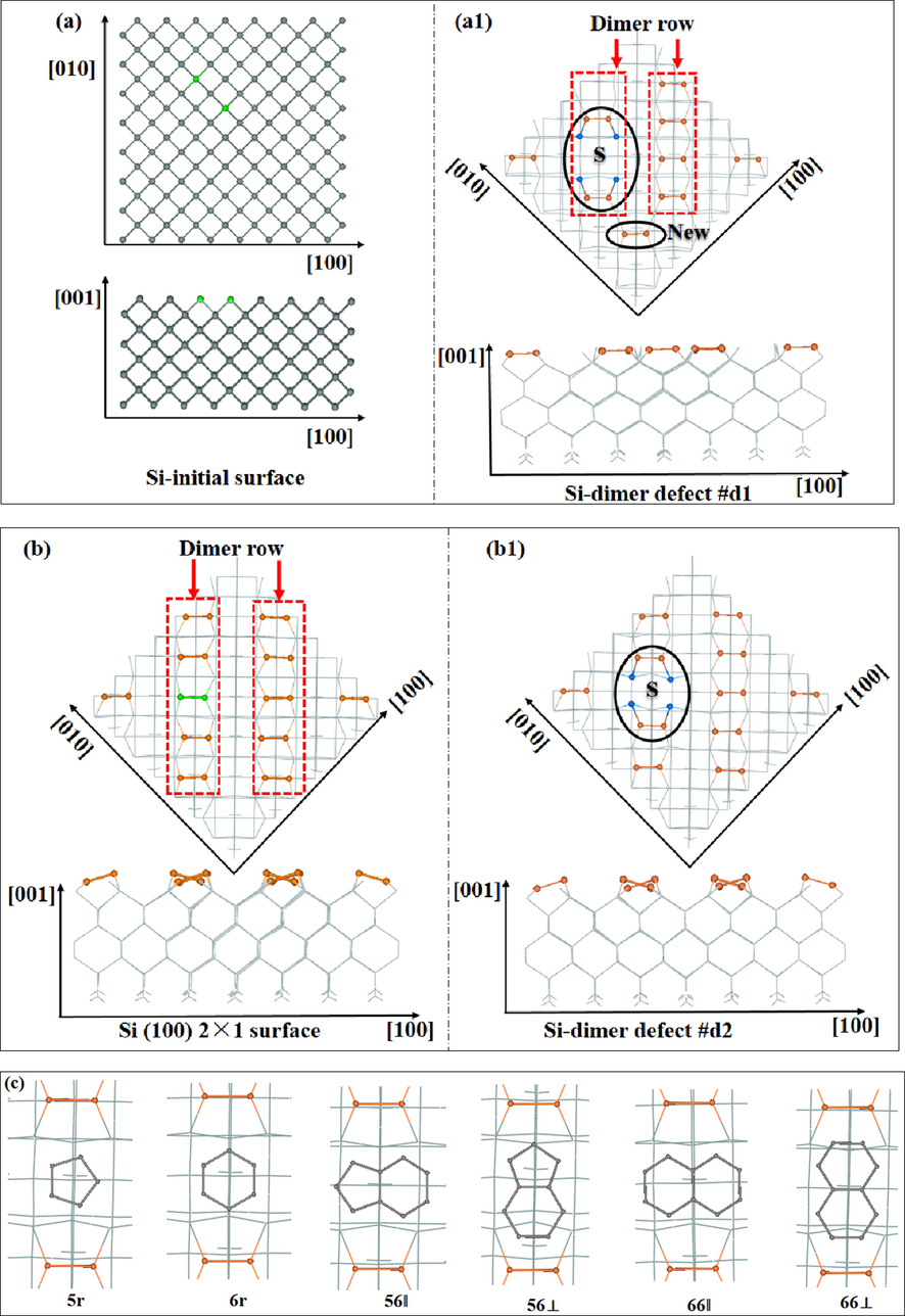
(a/a1) and (b/b1) correspond to two dimer defect surfaces, (c) is the six orientations of C60.
3 Results and discussion
3.1 Energy analysis
For the reconstructed Si(1 0 0) surface, the energy value of 0.31 eV for the removal of a single dimer to form a defective surface of type #d2 is slightly higher than the 0.28 eV reported in the study by Roberts et al (Roberts et al., 1994). For the C60 after geometry optimization through SCC-DFTB, the two characteristic C—C bond lengths are 1.41 Å and 1.45 Å respectively for shorter 6:6 ring bonds between the C atoms in adjacent hexagons, and longer 5:6 bonds between the atoms in adjacent pentagons and hexagons, which are consistent well with the experimental values of 1.40 Å and 1.45 Å, respectively (David et al., 1991). As listed in Table 2, the adsorption energy for 66‖ (2.8 eV) is fitful for the value of 2.8 eV in the reference. It can be noted that configuration 66‖ is also the most stable on the Si (1 0 0) 2 × 1 reconstructed surface in the reference (Hobbs et al., 2005), and this result is in good agreement with the adsorption energies obtained in other documents (Godwin et al., 2003). These prove the reliability of the current DFTB calculations. Fig. 2 shows the adsorption energy of twelve adsorption configurations. For #d1, the adsorption energies of 4.1 eV, 3.9 eV, and 3.8 eV for the 6r, 56‖, and 66⊥, respectively, suggesting that these adsorption configurations are more stable than others. Similarly, for #d2, configurations 6r, 56‖, and 66⊥with higher adsorption energies of 2.6 eV, 2.4 eV, and 2.3 eV. Obviously, the ability of dimer defect #d1 to bind C60 is significantly higher than that of #d2. Whether it is dimer defect #d1 or dimer defect #d2, configuration 6r is the most stable configuration, and the adsorption energy of 6r is also higher than 56‖. In order to qualitatively determine the distribution after adding dispersion correction, we performed a Lennard-Jones (L-J) dispersion correction for the adsorption energy of C60/Si(1 0 0) systems, where the dispersion energy can be added into the total energy in the present DFTB version as shown in Fig. 2 in green. As for #d1, a significant increase in adsorption energy can be observed for all configurations. At this time, the three conformations with the highest adsorption energy become d1-6r, d1-56‖, and d1-66⊥. As for#d2, the phenomenon of the increase in adsorption energy also occur after adding dispersion energy’s correction, where the three configurations with the highest binding energy become d2-6r, d2-56‖, and d2-66⊥, implying the importance of the van der Waals interaction for the molecular combined with Si(1 0 0).
Configurations
5r
6r
56‖
56⊥
66‖
66⊥
Ea/eV
0.7
0.2
1.4
0.8
2.8
0.6
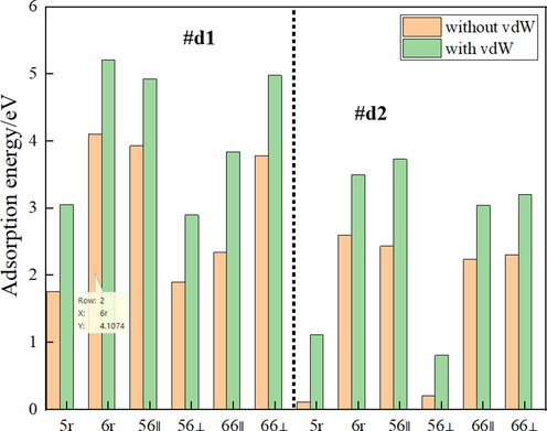
Adsorption energies for configurations, Orange and green correspond to without vdW and with vdW.
3.2 Structure analysis
The side view of the adsorption configuration and the partial top view of the C—Si bond mode after C60 adsorbed to the #d1-type silicon surface as shown in Fig. 3, in which each surface dimer with certain buckling is orange. Dimer atoms without any flexure at the same height along the [0 0 1] direction are shown in green, and blue silicon atoms are located in the second layer close to the defect. For the conformations of d1-5r, d1-6r, d1-56‖ and d1-66‖, when the surface dimer atoms are involved in the formation of the C—Si bond, it is a green dimer with the disappearance of flexion instead of an orange dimer with some flexion on the surface of the perfect Si(1 0 0)-(2 × 1). Green and orange dimers linked to blue silicon atoms in the d1-66‖ and d1-56‖ configurations can be observed, in addition, the bonding atoms are arranged asymmetrically, so the adsorption energy is obviously lower than that of in d1-6r, d1-56‖ and d1-66‖. Notably, the dimer buckling along the [0 0 1] direction disappears, when one or two atoms in the dimer connected to the blue silicon atom participate in the formation of the C—Si bond. According to the adsorption energy shown in Fig. 2, the ability of the #d1-type defective silicon surface to bind C60 is generally higher than the ability of the #d2-type defective silicon surface to bind C60. In the dimer row where the #d1-type adsorption in Fig. 1(a1). But for the #d2-type defective silicon substrate, the dimer row where the adsorption site is located not only exists outside the two dimers that participate in the formation of C-Si, but also has two other isolated dimers that do not participate in the formation of C-Si. In addition to the two dimers that are bonded, there are two additional isolated dimers that are not bonded to the C atom.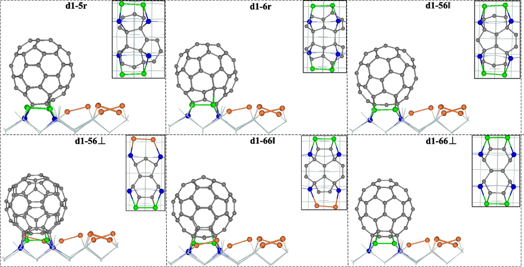
Configuration side view and partial bonding top view of C60 adsorbed to the #d1-type Si surface.
The side view of the configuration and the partially enlarged top view of the bonding atoms of C60 adsorbed to the #d2-type silicon surface are shown in Fig. 4. In conformation d2-56⊥, the orange dimer with flexure is directly attached to the blue silicon atom, while all other conformations are green dimers, and because the arrangement of the bonding atoms in the configuration d2-56⊥ is extremely asymmetric, the adsorption energy is the smallest.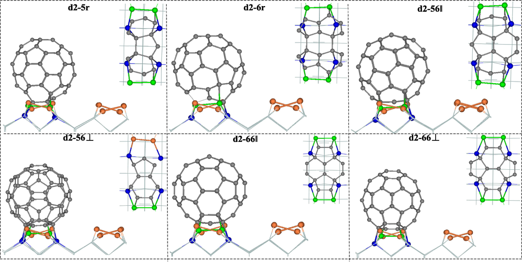
Configuration side and partialtop view of C60 adsorbed to #d2-type silicon surface.
The bonding patterns of the C60 with Si substrates, the C—Si bond length, and the partial bond length of C60 are given in Fig. 5. Here the Si and C atoms are marked in green and gray, and the C—Si and C—C bonds are marked in red and black. The surface and second layer Si atoms close to the defect are noted as Si1 and Si2 (shown in blue), respectively. The C—Si bond of d1-5r averages 2.07 Å. The 5:6 bond of the pentagonal ring located directly above the defect is significantly elongated from 1.45 Å to 1.62 Å, 1.65 Å, and 1.64 Å, and slightly elongated to 1.49 Å. The average bond length of the C—Si bond in the configuration d1-6r is 2.01 Å, where the 5:6 and 6:6 bonds of the hexagonal ring are elongated to 1.53 Å and 1.51 Å, respectively. The adsorption energy is also significantly higher than that of d1-5r due to the more symmetric bonding mode than d1-5r. Average bond length of the C—Si bond formed in the configuration d1-56‖ is 2.05 Å, the 5:6 and 66 bonds of C60 are elongated to 1.51 Å and 1.48 Å, respectively, and the other one is greatly shortened to 1.39 Å. For d1-56⊥, the adsorption energy is low due to the longer average C-Si bond and the low symmetry of the bonding mode. As shown in Fig. 1(a), due to the presence of a new dimer (marked with NEW) between the two rows of dimer, the d1-66‖ does not present an up-down mirror symmetry as that in d2-66‖. Although six C—Si bonds are formed, the patterns of those bonds is asymmetric, resulting in the adsorption energies significantly lower than that of in d1-6r and d1-56‖. For d1-66⊥, the average length of the eight C—Si bonds is 2.03 Å. Being similar to the configuration d1-5r, the four longer C—Si bonds formed from the hexagonal-hexagonal ring C atoms of C60 with Si2 are the average value 2.04 Å, while the two shorter outer C—Si bonds formed with Si1 atoms are 2.01 Å. In meanwhile, the 5:6 bond of C60 becomes 1.50 Å, while 6:6 bond is shortened to 1.36 Å, where these eight bonds are symmetrically distributed, resulting in a higher energy.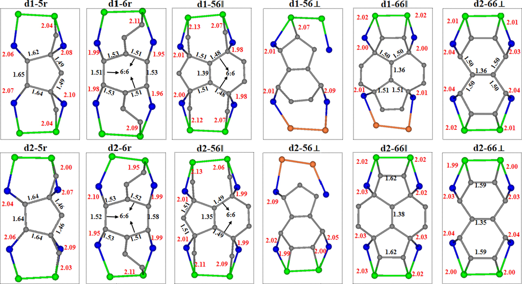
Top view of bonding atomic arrangement for C60 adsorbed to two dimer-defective Si surfaces.
For the case of #d2, when the pentagonal ring of C60 is located directly above the defect of Si substrate, the average bond length of the C—Si bond formed by the four C atoms in the pentagonal ring with Si2 is 2.07 Å. The 5:6 bond of C60 is stretched from 1.45 Å to 1.64 Å and 1.46 Å, respectively. Due to the large deformation of the pentagonal ring in C60, the adsorption energy of the configuration d2-5r is very low. The average C—Si bond length in d2-6r is 2.01 Å. The 5:6 bond of the hexagonal ring where the bonded carbon atoms are located is stretched to 1.53 Å and 1.58 Å (the 6:6 bond becomes 1.52 Å). The adsorption energy is significantly higher than that of d2-5r because of the smaller deformation and more symmetric bonding pattern. The average C-Si bond length in the configuration d2-56‖ is 2.05 Å. The 5:6 bond of C60 is elongated to 1.51 Å and the other is shortened considerably to 1.35 Å (The 6:6 bond is elongated from 1.41 Å to 1.49 Å). The adsorption energy is low because of the asymmetric presence of C-Si bond at d2-56⊥. The average C—Si bond lengths of the configurations d2-66‖ and d2-66⊥ are 2.02 Å and 2.01 Å, respectively. The 6:6 bond lengths (1.38 Å) and 5:6 bond lengths (1.50 Å) of d2-66‖ are longer than those of d2-66⊥ (1.35 Å) and 5:6 bond lengths (1.49 Å), so the adsorption energy of the former is lower than that of the latter.
3.3 Differential charge density and Mulliken population
The charge density differences of the configurations d1-6r, d2-6r, d1-56‖ and d2-56‖ with higher adsorption energy are shown in Fig. 6, where blue and yellow indicate negative and positive charge densities, respectively. After adsorption, the charge accumulation between C60 and the Si substrate indicated that the carbon and silicon atoms were bound by covalent bonds. Whether C60 is adsorbed on a #d1 or #d2 dimer-deficient silicon substrate, the binding atoms come mainly from the silicon atoms on the surface and the carbon atoms on the bottom of the C60 near the silicon substrate. At the same charge density threshold scale, the negative blue charge density of C60 is uniformly distributed in configurations d1-6r, while in configurations d2-6r it is concentrated along the z-direction at the top and near the bottom of the silicon substrate, and a relatively large amount of positive yellow charge density appears at the bottom. The different placement orientations of C60 molecules with respect to the silicon substrate have a significant effect on the charge accumulation region. It is noteworthy that when the pentagon-hexagonal ring of C60 is flush with the silicon substrate, there is a significant positive charge density accumulation at the bottom of C60 in configurations d1-56‖ and d2-56‖.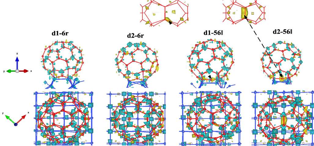
Charge differential density of d1-6r, d2-6r, d1-56‖, and d2-56‖.
Mulliken charge of surface atoms after adsorption of #d1-type Si substrate is shown in Fig. 7. The red dashed boxes in the figure indicate the surface silicon atoms near the defects, labeled Si11, Si12, Si13 and Si14, respectively as shown in configuration d1-5r. The corresponding local magnified side view shows the green dimer without flexure, while the orange dimer still maintains some flexure. In the configurations d1-5r and d1-6r, Si11 and Si12 are involved in the formation of C—Si bonds and have a Milliken charge of 4.0. However, Si13 and Si14 are not involved in the formation of C—Si bonds and accept charge (Si13 > Si14). In the configurations d1-56‖ and d1-66⊥, Si11, Si12, Si13 and Si14 are all involved in the formation of C—Si bonds and the Milliken charge are all of 4.0. In the configurations d1-56⊥ and d1-66‖, Si12 and Si13 are not involved in the formation of C—Si bonds, where Siu is neutral (top and side views are marked with black double-arrow dashed lines) and Sid loses charge; this is not consistent with the perfect Si(1 0 0)-(2 × 1) surface dimer in which Siu is richly charged and Sid is undercharged. Here, it can be found that when both silicon atoms of the dimer are involved in the formation of C—Si bonds, they become neutral and the dimer in which they are located disappears in flexion.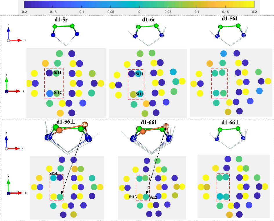
Mulliken charge of surface atoms after adsorption of #d1-type Si substrate.
For the case of #d2 type silicon substrates, Mulliken charge of surface atoms after adsorption of #d2-type Si substrate are shown in Fig. 8. In the configurations d2-5r and d2-6r, Si11 and Si12 are involved in the formation of C—Si bonds and are close to neutral in charge. Si13 and Si14 are not involved in the formation of C—Si bonds and gain charge in different degrees. In the configurations d2-56‖, d2-66‖ and d2-66⊥, Si11, Si12, Si13 and Si14 are involved in the formation of C—Si bonds with charges close to neutral. In the configuration d2-56⊥, Si11 and Si14 are not involved in the formation of C—Si bonds, and the dimers in which they are located have some degree of flexure, where Siu is electron-rich and Sid electron-deficient, which is similar to the dimer on Si(1 0 0)-(2 × 1) before adsorption.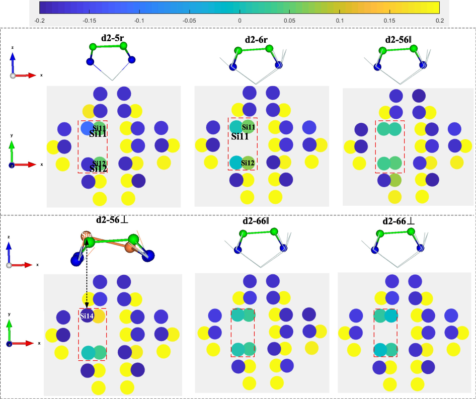
Mulliken charge of surface atoms after adsorption of #d2-type Si substrate.
Fig. 9 visually shown the Mulliken charge on the atom for the bonding atoms. Here, if the net charge on any atom is less than 0.0, it indicates that the atom accept electrons, otherwise it donate electrons. In this figure, Si atoms in the substrate are represented by larger green spheres, while C atoms are represented by relatively small gray spheres, and each pair of C—Si bonds are marked with arrows. The formed C—Si bonds are marked with numbers b1-b8, respectively. For the configurations d1-6r, d2-6r, d1-56‖, and d2-56‖, the Si atoms always donate electrons and the C atoms gain charge in the formed C—Si bonds. The shorter the C—Si bond length, the more obvious the charge transfer.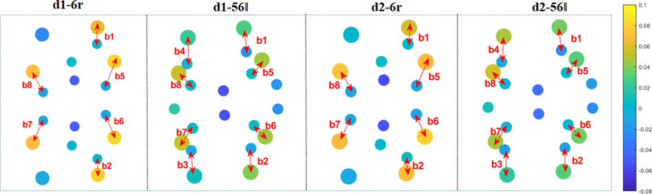
Top view of the locally bonded Mulliken charges of configurations d1-6r, d2-6r, d1-56‖, and d2-56‖.
The net charge of the atoms in each C—Si bond pair, the bond energy, and the number of Mulliken electron bureaus in the atomic orbitals are listed in Table 3. After adsorption, the charge were transferred from the silicon atoms in the substrate to the carbon atoms in C60, which reflects the difference in electronegativity between them. For the relatively short C—Si bonds (b5, b6, b7 and b8) in the conformations d1-6r and d2-6r, the 3 s orbital number of silicon atoms decreases while the 3p increases slightly, with an average net charge of −0.08. Similarly, the 3s and 3p orbitals of Si atoms in the relatively short C—Si bonds (b5, b6, b7, and b8) in the d1-56‖ and d2-56‖ configurations show little variation, and their average net charge of −0.06 is higher than that of the longer C—Si bonds (b1, b2, b3, and b4) with an average net charge of −0.03. In contrast, the 2s and 2p orbitals on the carbon atoms involved in the formation of C—Si bonds and the net charge changes are small.
Bond energy/eV
Si
C
3s
3p
net charge
net charge
2s
2p
d1-6r
b1/0.21
1.56
2.38
−0.06
0.00
1.24
2.76
d2-6r
b2/0.31
1.57
2.37
−0.06
0.01
1.24
2.77
b5/0.31
1.50
2.41
−0.09
0.01
1.24
2.77
b6/0.22
1.50
2.42
−0.08
−0.01
1.23
2.76
b7/0.29
1.49
2.42
−0.09
0.01
1.24
2.77
b8/0.29
1.50
2.43
−0.07
0.01
1.24
2.77
b1/0.21
1.57
2.37
−0.06
−0.01
1.23
2.76
b2/0.31
1.58
2.36
−0.06
0.01
1.24
2.77
b5/0.31
1.50
2.42
−0.08
0.01
1.24
2.77
b6/0.21
1.51
2.41
−0.08
−0.01
1.23
2.76
b7/0.29
1.49
2.44
−0.07
0.01
1.24
2.77
b8/0.29
1.49
2.43
−0.08
0.01
1.24
2.77
d1-56‖
b1/0.22
1.51
2.45
−0.04
0.02
1.24
2.78
b2/0.27
1.50
2.46
−0.04
0.00
1.23
2.77
b3/0.26
1.50
2.45
−0.05
−0.01
1.23
2.76
b4/0.22
1.51
2.46
−0.03
0.01
1.24
2.77
b5/0.21
1.51
2.43
−0.06
0.01
1.24
2.77
b6/0.26
1.50
2.44
−0.06
−0.01
1.23
2.76
b7/0.26
1.51
2.44
−0.05
−0.01
1.23
2.76
b8/0.20
1.50
2.44
−0.06
0.00
1.24
2.76
d2-56‖
b1/0.23
1.55
2.41
−0.04
0.02
1.24
2.78
b2/0.26
1.50
2.47
−0.03
−0.01
1.23
2.76
b3/0.26
1.50
2.46
−0.04
0.00
1.24
2.76
b4/0.21
1.51
2.45
−0.04
0.01
1.24
2.77
b5/0.21
1.51
2.44
−0.05
0.02
1.25
2.77
b6/0.26
1.50
2.45
−0.05
0.00
1.24
2.76
b7/0.25
1.52
2.42
−0.06
0.00
1.24
2.76
b8/0.20
1.51
2.43
−0.06
0.01
1.24
2.77
3.4 Chemical potential
The chemical potential is the fermi energy at 0 K. The chemical potential of C60 adsorbed on the dimer-deficient Si(1 0 0) surface is shown in Fig. 10. The chemical potential for C60 adsorption on #d1-type defective silicon substrates is significantly higher than that of in #d1-type defective silicon substrates. The higher chemical potential of the configuration d1-56⊥and d2-56⊥indicates the high oxidation reaction activity with strong electron giving ability, while the lower chemical potential of the configuration d1-66⊥and d2-66⊥indicates the high reduction reaction activity with weak electron giving ability.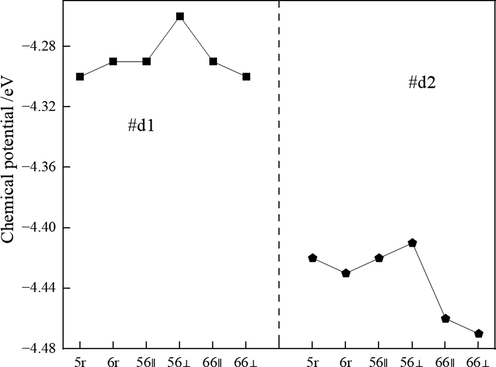
Chemical potential of configurations.
4 Conclusions
In this paper, SCC-DFTB calculations were performed to investigate the adsorption C60 onto the reconstructed Si(1 0 0) surface having two types of missed dimers. The four silicon atoms of the surface and second layer adjacent to the defect are involved in the formation of C—Si bonds. The larger hexagonal ring of C60 is more easily bonded to the silicon substrate to form a stable structure compared to the other orientations of C60, where a charge accumulation region exists between the silicon substrate and C60 in configuration with higher adsorption energy. Mulliken charges on the atoms in dimers and dimer’s flexure are altered due to the formation of C—Si bonds. The charge transfer is more pronounced in the shorter C—Si bond, and the C atoms are all relatively negative in charge, while silicon atoms are all positive, increasing the attraction between the two kinds of atoms as well as the stability of the structure.
Acknowledgments
Project supported by the National Natural Science Foundation of China (Grant No. 51671051)
Declaration of Competing Interest
The authors declare that they have no known competing financial interests or personal relationships that could have appeared to influence the work reported in this paper.
References
- Growth of C60 fullerene films on semiconductor surfaces. Mrs Proc.. 2003;768:75-80.
- [CrossRef] [Google Scholar]
- Tuning electronic properties of semiconductors by adsorption of [60]Fullerene carboxylic acid derivatives. Adv. Mater.. 2002;14:802-805.
- [CrossRef] [Google Scholar]
- Comprehensive study of the encapsulation of Lomustine anticancer drug into single walled carbon nanotubes (SWCNTs): Solvent effects, molecular conformations, electronic properties and intramolecular hydrogen bond strength. J. Molecular Liq.. 2020;320 Part A:114285.1-114285.7.
- [CrossRef] [Google Scholar]
- Redox-active Si(100) surfaces covalently functionalised with [60]fullerene conjugates: new hybrid materials for molecular-based devices. J. Mater. Chem.. 2008;18:1570-1581.
- [CrossRef] [Google Scholar]
- First-principles investigation of C60 molecule adsorption on a diamond (100)-2×1 surface. Model Simul. Mater. Sci. Eng.. 2011;19:045001.1-045001.11.
- [CrossRef] [Google Scholar]
- Optical properties in 1D photonic crystal structure using Si/C60 multilayers. J. Semicond.. 2009;30(4):5-7.
- [CrossRef] [Google Scholar]
- Atomic and electronic imaging of semiconductor surfaces with scanning tunneling microscopy. Am. Inst. Phys. AIP. 1987;160:496-505.
- [CrossRef] [Google Scholar]
- An STM study of C60 adsorption on Si(100)-(2×1) surfaces: from physisorption to chemisorption. Surf Sci. 1995;329
- [CrossRef] [Google Scholar]
- Nanoscale Science of Single Molecules Using Local Probes. Science. 1999;283:1683-1688.
- [CrossRef] [Google Scholar]
- The structure of C60 and endohedral C60 on the Si(100) surface. Surf. Sci.. 2001;490:409-414.
- [CrossRef] [Google Scholar]
- The bonding sites and structure of C60 on the Si(100) surface. Surf. Sci.. 2003;529:237-246.
- [CrossRef] [Google Scholar]
- Determination of the local electronic structure of atomic-sized defects on Si(001) by tunneling spectroscopy. J. Vac. Sci. Technol. A. 1989;7(4):2854-2859.
- [CrossRef] [Google Scholar]
- Fullerene-based electron-spin quantum computer. Phys. Rev. A. 2002;65:184.
- [CrossRef] [Google Scholar]
- An ab initio study of C60 adsorption on the Si(001) surface. Surf. Sci.. 2005;591:45-55.
- [CrossRef] [Google Scholar]
- DFTB+, a software package for efficient approximate density functional theory based atomistic simulations. J. Chem. Phys.. 2020;152:124101.1-124101.13.
- [CrossRef] [Google Scholar]
- Bond breaking coupled with translation in rolling of covalently bound molecules. Phys. Rev. Lett.. 2005;94(14):146104.1-146104.4.
- [CrossRef] [Google Scholar]
- Photovoltage generation of Si/C60 heterojunction. J. Appl. Phys.. 1996;79(5):2798-2800.
- [CrossRef] [Google Scholar]
- Structure and bonding nature of C60/Si(100)-c(4×4): density-functional theory calculations. Phys. Rev. B. 2007;7:25305.1-25305.5.
- [CrossRef] [Google Scholar]
- Adsorption structure of a single C60 molecule on Si(111)-(7×7): density-functional calculations. Surf. Sci.. 2008;602:1408-1412.
- [CrossRef] [Google Scholar]
- Strain acting on adsorption of C60 onto graphene from DFTB algorithm. Carbon Trends. 2021;5:100138.1-100138.9.
- [CrossRef] [Google Scholar]
- C60 adsorption on Si(100) 2×1 reconstructed surface with single vacancy in sub-surface from DFTB algorithm. Mater. Sci. Semicond. Process. 2022;144:106625.1-106625.11.
- [CrossRef] [Google Scholar]
- Investigating the effect of electric field on the adsorption of C60 onto graphene from density functional tight-binding simulations. Diamond Related Mater.. 2022;125:109008.1-109008.9.
- [CrossRef] [Google Scholar]
- Chem. Eng. J.. 2022;428(15):131991.1-131991.14.
- [CrossRef]
- Shearing bridge bonds in carbon nitride vesicles with enhanced hot carrier utilization for photocatalytic hydrogen production. Cat. Sci. Technol.. 2022;12:4193-4200.
- [CrossRef] [Google Scholar]
- Design of a high-performance graphene/SiO2-Ag periodic grating/MoS2 surface plasmon resonance sensor. Appl. Opt.. 2022;61(23):6752-6760.
- [CrossRef] [Google Scholar]
- High-yield aqueous synthesis of partial-oxidized black phosphorus as layered nanodot photocatalysts for efficient visible-light driven degradation of emerging organic contaminants. J. Cleaner Product.. 2022;377(1):134228.1-134228.14.
- [CrossRef] [Google Scholar]
- Organic functionalization at the Si(001) dimer vacancy defect-structure, bonding, and reactivity. J. Phys.Chem C. 2021;125:5635-5646.
- [CrossRef] [Google Scholar]
- An overview of molecular layer deposition for organic and organic-inorganic hybrid materials: mechanisms, growth characteristics, and promising applications. J. Mater.Chem A. 2017;5:18326-18378.
- [CrossRef] [Google Scholar]
- Mizuseki, H., Sahara, R., Hongo, K., 2021. Order-Disorder competitive cooperation in equiatomic 3D-Transition-Metal quaternary alloys: phase stability and electronic structure 22,62-67. .
- Adsorption geometries and interface electronic structure of C60 on Si(100)2 × 1 reconstruction surface. Surf. Sci.. 2019;690(3):121484.1-121484.5.
- [Google Scholar]
- DFT study of ozone dissociation on BC3 graphene with Stone-Wales defects. J Mol Model. 2014;20:2071.
- [CrossRef] [Google Scholar]
- Influence of antisite defect upon decomposition of nitrous oxide over graphene-analogue SiC. Thin Solid Films. 2014;552:111-115.
- [CrossRef] [Google Scholar]
- Rational design of asymmetric atomic Ni-P1N3 active sites for promoting electrochemical CO2 reduction. Nano Res.. 2022;15(12):1-7.
- [CrossRef] [Google Scholar]
- Estimation of fetal volume by magnetic resonance imaging and stereology. Br. J. Radiol.. 1994;67(803):1067-1077.
- [Google Scholar]
- Density functional theory for a model quantum dot: beyond the local-density approximation. Phys. Rev.. 2011;83(11):115128.1-115128.8.
- [CrossRef] [Google Scholar]
- Epitaxial silicon overgrowth of C60 on the Si(100)-2×1 surface. Surf. Sci.. 2008;602:493-498.
- [CrossRef] [Google Scholar]
- Role of coverage and vacancy defect in adsorption and desorption of benzene on Si(001)-2×n surface. Bull Korean Chem. Soc.. 2010;31:162-167.
- [CrossRef] [Google Scholar]
- Organic and inorganic-organic thin film structures by molecular layer deposition: a review. Beilstein J. Nanotechnol.. 2014;5:1104-1136.
- [CrossRef] [Google Scholar]
- Atomic Force Microscopy (AFM) Curr. Protoc. Microbiol.. 2008;8:2C.2.1-2C.2.17.
- [CrossRef] [Google Scholar]
- Dimer vacancies and dimer-vacancy complexes on the Si(100) surface. Phys. Rev. B. 1993;47(16):10497-10508.
- [CrossRef] [Google Scholar]
- Porous Organic Polymer-Derived Nanopalladium Catalysts for Chemoselective Synthesis of Antitumor Benzofuro[2,3-b]pyrazine from 2-Bromophenol and Isonitriles. Org. Lett.. 2019;21(13):4929-4932.
- [CrossRef] [Google Scholar]
- Predicted a honeycomb metallic BiC and a direct semiconducting Bi2C monolayer as excellent CO2 adsorbents. Chin. Chem. Lett.. 2022;33(5):2595-2599.
- [CrossRef] [Google Scholar]
- Influence of topological defects on the nitrogen monoxide-sensing characteristics of graphene-analogue BN. Sens. Actuators B. 2014;197:274-279.
- [CrossRef] [Google Scholar]
- Chemisorption of small fullerenes Cn(n=28,32,36,40,44,48,60) on the Si(001)-c(2×1) surface. Phys. Rev. B. 2009;79:155304.1-155304.13.
- [CrossRef] [Google Scholar]
- Nanocarrier for levodopa Parkinson therapeutic drug; comprehensive benserazide analysis. Artificial Cells, Nanomed., Biotechnol.. 2018;46(sup1):434-446.
- [CrossRef] [Google Scholar]
- Carboxylated single-walled carbon nanotubes as a semiconductor for adsorption of acrylamide in mainstream cigarette smoke. Phys. E Low-dimensional Syst. Nanostruct.. 2020;124:114299.1-114299.6.
- [CrossRef] [Google Scholar]
- Palladium-Doped single-walled carbon nanotubes as a new adsorbent for detecting and trapping volatile organic compounds: a first principle study. Nanomaterials. 2022;12(15):2572.1-2572.11.
- [CrossRef] [Google Scholar]
- Physical properties and chemical reactivity of the buckled dimer on Si(100). Prog. Surf. Sci.. 2004;77:37-70.
- [CrossRef] [Google Scholar]
- Fullerene-C60 and crown ether doped on C60 sensors for high sensitive detection of alkali and alkaline earth cations. Phys. E: Low-dimensional Syst. Nanostruct.. 2017;87:51-58.
- [CrossRef] [Google Scholar]
Appendix A
Supplementary material
Supplementary data to this article can be found online at https://doi.org/10.1016/j.arabjc.2023.104816.
Appendix A
Supplementary material
The following are the Supplementary data to this article:Supplementary data 1
Supplementary data 1