

Translate this page into:
A Comprehensive Study on Structural and Optical Properties of Zinc Selenide/Poly Ortho-methoxyaniline Hybrid Thin Films Deposited by Chemical Bath Deposition and Plasma Polymerization Techniques
⁎Corresponding author at: Department of Physics, Bangladesh University of Engineering and Technology, Dhaka 1000, Bangladesh. mjrahman@phy.buet.ac.bd (Mohammad Jellur Rahman)
-
Received: ,
Accepted: ,
This article was originally published by Elsevier and was migrated to Scientific Scholar after the change of Publisher.
Abstract
Hybrid thin films hold dominant importance in various technological applications due to their synergistic effects between inorganic and organic materials. In this study, inorganic–organic hybrid thin film has been produced where the inorganic layer of zinc selenide (ZnSe) is deposited first through chemical bath deposition technique and the organic layer is deposited onto the inorganic layer using a capacitively coupled plasma polymerization technique. The ZnSe layer deposited for one hour has been used as the base layer and plasma polymerized (PP) o-methoxyaniline (OMA) has been deposited for different deposition durations. The experimental results showed that thickness of the the hybrid films increases with the organic layer deposition time. The field emission scanning electron microscope exhibited a large number of pores on the surface of the ZnSe film, which are significantly covered up when organic PPOMA is deposited onto it. The energy-dispersive X-ray confirms the constitutional elements of the hybrid films and X-ray diffraction study indicates the enhancement of crystallinity of the film. Differential scanning calorimetry and thermogravimetric analysis specify that hybrid films are thermally more stable (up to 396 °C) compared to pure ZnSe film (351 °C), probably due to higher conjugation in the PP organic layer. The direct optical band gaps of the deposited hybrid thin films are found to increase from 2.4 to 2.80 eV with the increase of organic layer onto ZnSe film. Consequently, the Urbach energy decreases from 0.94 to 0.66 eV with the deposition of hybrid film for different time durations. The outcomes of this study suggest that the hybrid films would have enormous potential as passive thin films for photovoltaic cells, sensing and optical devices.
Keywords
Ortho-methoxyaniline
Zinc selenide film
Plasma polymerization
Chemical bath deposition
Hybrid thin films

1 Introduction
The intriguing properties and simple structure of inorganic–organic hybrid thin films have garnered significant interest. Such films are used in a wide range of applications in optoelectronics and energy storage devices, sensors, thin film transistors, and solid-state lighting systems (Kannichankandy et al., 2020; Yen et al., 2020; Zang et al., 2021). Organic materials generally exhibit constraints including weak mechanical toughness, inadequate thermal stability, and restricted charge transport capabilities. Conversely, inorganic materials, encompassing metals, metal oxides, and semiconductors present superior mechanical strength, thermal stability, and proficient charge transport properties (Wang et al., 2013; Lee et al., 2019). Since the hybrid film uniquely blends the various properties of both organic and inorganic materials into a single personalized structure, inorganic–organic hybrid thin films play a vital part in materials science and modern technology (Li et al., 2018; Reddy et al., 2019). This cooperative combination provides an opportunity to create materials with enhanced performance properties that exceed the separate capacities of each material group, whether it is to increase sensor sensitivity, achieve mechanical robustness in flexible electronics, or maximize photovoltaic cell energy conversion efficiency. These hybrid films provide an adaptable basis for creative endeavors (Nyabadza et al., 2021). Moreover, they exhibit potential for the actualization of commercially feasible production procedures, making them essential components in the development of state-of-the-art technologies across a broad range of industries, including electronics, energy conversion, and sensing applications (Saadiah et al., 2019). Therefore, by integrating inorganic and organic materials, hybrid thin films would emerge as a smart solution transcending individual limitations and intertwining distinct properties for enhanced functionality.
Chemical bath deposition (CBD) has been used extensively in thin film deposition due to its versatility, cost-effectiveness, and ability to produce uniform coatings on a variety of substrates (Soonmin, 2016; Kariper, 2016). CBD is particularly valuable for applications requiring low-temperature processing and complex geometries. It offers precise control over film properties through adjustments in bath composition and deposition parameters, making it ideal for tailoring materials to specific needs (Thirumavalavan et al., 2016; Darafarin et al., 2016). On the other hand, plasma polymerization process is a highly versatile technique getting smooth, pinhole free and homogeneous thin films which are suitable for various applications like protective coatings and biomedical devices (Akther et al., 2022). This method is an attractive sustainable alternative to thin film deposition for both research and commercial applications because it never needs a solvent or initiator to begin the deposition process and produces no harmful byproducts (Sheikh et al., 2023; Akther et al., 2023).
Plenty of studies have been done investigating different properties of organic or inorganic thin films using both plasma polymerization and CBD techniques. However, the research on organic–inorganic hybrid thin film using two different methods is scanty in the literature. Only a few works on composite or hybrid thin films are reported in the literature which are deposited with more than one deposition technique [4–6]. Wang et al. showed the drawbacks of various single organic or inorganic sensing materials restricted in their practical field of applications. They proposed that the organic/inorganic hybrid materials with improved performances can recover those limitations enhancing the sensor performances, such as repeatability, stability, and recovery speed. In this case, inorganic compounds generally have high chemical and thermal stability that allows them to operate under different harsh conditions whereas organic compounds make it possible to modify the molecular structure of the sensing materials to elevate the selectivity toward a target analyte (Wang et al., 2013). Jin et al. (Jin and Wang, 2013) reported hybrid thin film photoconductors combining organic–inorganic components to achieve exceptional responsivity. In this hybrid device, the organic component serves as superior light-absorbing capabilities and generates free charge carriers, while the inorganic component facilitates efficient electron transport to optimize overall device performance. In some studies, researchers also showed the importance of hybrid thin films with various tunable optical and structural properties (Jo et al., 2019; Lee et al., 2020; Hassanien et al., 2016).
In this study, zinc selenide (ZnSe) and o-methoxyaniline (OMA) have been chosen to produce the hybrid thin films, because ZnSe film exhibits excellent chemical stability and possesses a direct wide bandgap of 2.67 to 2.90 eV coupled with high optical transparency. Notably, this energy band gap can be effectively tuned across a wide range in both the visible and infrared regions by varying different deposition parameters (Chowdhury et al., 2017; Toma et al., 2021). ZnSe thin films are mostly prepared by the CBD methods owing to have various advantages discussed in different research works (Thirumavalavan et al., 2016; Tezel and Kariper, 2019). These unique combinations of properties make ZnSe film a decisive material for various applications such as a window layer in thin film solar cells (Chowdhury, 2017) and biological sensors, and also a promising candidate for getting hybrid thin film (Muntaz, 2016). Besides these, OMA is a cost-effective monomer that readily offers several advantages in the fabrication of electronic and optoelectronic devices like organic thin film transistors and organic light-emitting diodes (Badran et al., 2016). Plasma polymerized (PP) OMA thin films are generally smooth, homogeneous, and pinhole-free, which have potential applications in various optoelectronic devices (Rahman and Bhuiyan, 2013). By combining ZnSe and PPOMA as a hybrid structure, may create some specific tailored advantages like tunable optical properties, improved thermal and mechanical stability, material versatility, and overall enhanced device performances.
This study presents a novel approach to fabricating hybrid thin films with improved structural properties, surface morphology, thermal stability, and tunable optical properties. The absorption is tuned by adjusting the deposition time of the PPOMA organic layer. This tunability of different properties of hybrid films is important for specific application requirements. The results of this study may contribute to the field of materials engineering and provide possible advancement for the development of future electronic, optoelectronic, and high-sensing devices.
2 Materials and methods
Sodium sulfate (Anhydrous) (Na2SO4), zinc acetate (ZnC4H2O4), selenium powder (Se), and ammonia solution (NH4OH) with purities of 98 %, 99.5 %, and 37 % respectively, are collected from BDH, England. Hydrazine hydrate (N2H4) and acetone (C3H6O) of purities 100 % and 99.9 %, respectively are collected from Merck, Germany. Sodium hydroxide (NaOH) of purity 100 % is collected from DLab Chemicals, India. The organic precursor OMA is purchased from BDH Chemicals Ltd., Poole, England in liquid form, whose molecular structure is shown in Fig. 1.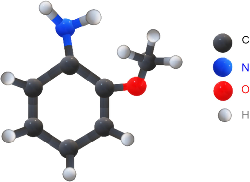
Chemical structure of OMA.
At first, locally purchased glass substrates (1.2 * 25.4 * 76.2 mm3, Sail brand, China) were first cleaned with mild soap water, followed by acetone degreasing, 5 % HCl etching for 30 min, ultrasonically cleaning with de-ionized water, and finally air-dring (Sheikh et al., 2023).
In order to prepare ZnSe film, firstly sodium selenosulfate (Na2SeSO3) solution is obtained by reacting 4.73 g of Se metal powder with 7.56 g of Na2SO3 in 200 ml of DI water and keeping the solution in rest for 9 h at 90 °C. After cooling overnight, it was filtered to obtain a clear light-yellow Na2SeSO3 solution. 1 M 60 ml aqueous solution of (Zn (CH3CO2)2) was taken in a 250 ml beaker and mixed with 45 ml of N2H4 while stirring continuously. Following that, liquor ammonia was introduced drop by drop while being constantly stirred. Due to the production of Zn(OH)2, the solution at first seemed hazy. The solution was clear and transparent due to the dissolved white Zn(OH)2 precipitate as well as the excess ammonia. The pH of the solution was reduced to 11 adding 1 M, 30 ml NaOH in it. Then 60 ml of prepared Na2SeSO3 solution was added into it. The chemical bath was placed on hotplate and at 80 °C a pre-clean glass substrate was dipped vertically into the solution. At that time the solution was rotating at a speed of 90 ± 2 rpm. After one hour of deposition, the substrate was removed from the beaker, washed with distilled water, and dried in open air. Afterward, the films are annealed at 300 °C for 1 h and kept for the deposition of organic film onto it.
To obtain ZnSe/PPOMA hybrid film the annealed ZnSe thin film was allowed to deposit the PPOMA layer using the plasma polymerization technique. The deposition process has been thoroughly explained in a previous study (Sheikh et al., 2023). The plasma chamber consists of two parallelly placed electrodes made of stainless steel to create a uniform electric plasma field. A rotary pump was used to vacuum the plasma chamber to a low pressure of 0.1 Torr. The electrodes were powered by a 42 W AC (50 Hz) power source to generate a discharge plasma glow. The vapor of the OMA connected with the vacuum chamber entered into the plasma reactor because of the high-pressure difference between the chamber and the monomer container. The injecting valve controlled the flow rate (∼20 cm3/min) to get uniform plasma deposition. The PPOMA layers on the ZnSe film were deposited for 30, 45, and 60 min and the respective hybrid film was identified by ZnSe/PPOMA_30, ZnSe/PPOMA_45, and ZnSe/PPOMA_60, respectively. The pure ZnSe film annealed for 1 h was named as ZnSe/PPOMA_00.
The thicknesses, d, of the as-deposited hybrid film, are measured using a multiple-beam interferometric technique (Tolansky, 1948) with the help of Eq. (1).
where λ = 589.3 nm for sodium light and is the fringe of interfaces. Details of thickness measuring procedures using this interferometric technique are described in an earlier research (Sarder et al., 2022). The thickness of the pure ZnSe film (ZnSe/PPOMA_00) was found to be 373 ± 7 nm and the width of this layer in the hybrid film remained almost constant. When the layer of PPOMA film onto the ZnSe layer deposited for 30, 45, and 60 min the corresponding thickness of the hybrid films ZnSe/PPOMA_30, ZnSe/PPOMA_45, and ZnSe/PPOMA_60 was found to be 415 ± 3, 494 ± 5 and 540 ± 4, in where the thickness of the PPOMA layer is approximately 42, 121 and 167 nm, respectively.
2.1 Characterization techniques
The as-deposited hybrid film surface was inspected by field emission scanning electron microscope (FESEM) (JEOL JSM 7600F, USA) at an accelerating voltage of 15 kV. Energy dispersive X-ray (EDX) was linked with FESEM to obtain the elemental data. The XRD patterns of the films were obtained by an X-ray diffractometer (Bruker, D8 Advance) using CuKα radiation (λ = 1.5406 Å). The thermal stability of ZnSe/PPOMA films under N2 atmosphere was examined by a computer-controlled thermogravimetric analyzer (TGA) and differential scanning calorimetry (DSC) (NETZSCH STA 449 F3 Jupiter). The analyzer employs a horizontal system balance mechanism (heating rate = 10 °C/min). A dual-beam UV–vis spectrometer coupled with an integrating sphere (SHIMADZU UV-2600, Japan) was employed to measure the optical parameters (absorbance, A, and transmittance, T) in the wavelength range of 200 – 700 nm, and absorption coefficient (α), optical band gap energy (Eg) and Urbach energy (EU) were found from these. A pre-cleaned glass substrate was used as a reference.
3 Results and discussion
3.1 Surface morphology
FESEM is the most widely used technique to observe the surface morphology of any as-deposited thin films. In this study FESEM images of the hybrid film surface were recorded at 50 K magnification with an accelerating voltage of 15 kV, which is shown in Fig. 2. The FESEM micrograph of ZnSe/PPOMA_00 film shows a rougher surface with a fiber-type structure. Similar characteristics were also noted in previous studies (Hile et al., 2020; Wei et al., 2013). Some agglomerates are formed on the film surface, which may be owing to the combination or fuse of some grains during the ZnSe film formation (Sadekar et al., 2013). After the deposition of PPOMA onto the ZnSe film surface, the hybrid film surface becomes smooth and the fiber-type structure completely disappears due to being covered up by the PPOMA layer. This improvement on the hybrid film surface is notably observed due to the increase of the PPOMA layer with the increase of deposition time. Generally, the PPOMA film deposited by the plasma polymerization technique is smooth, pinhole-free, and homogeneous (Rahman and Bhuiyan, 2013). However, due to having a rougher surface on the pure ZnSe film the hybrid film surface is also observed to be slightly bumpy. The formation of layer-by-layer hybrid film is confirmed from the cross-sectional view of a film as shown in Fig. 2 (e). These types of hybrid films would enhance the device performances of various optoelectronics devices (Jin and Wang, 2013).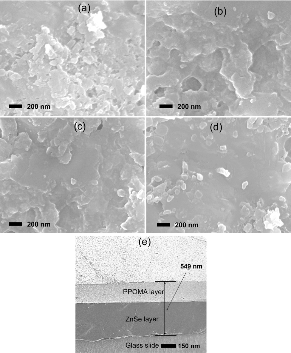
FESEM images of (a) ZnSe/PPOMA_00, (b) ZnSe/PPOMA_30, (c) ZnSe/PPOMA_45, (d) ZnSe/PPOMA_60 films, (e) Cross-sectional view of the ZnSe/PPOMA_60 hybrid film.
3.2 Elemental study
The constitutional elements of the as-deposited ZnSe/PPOMA hybrid thin films were determined with the help of EDX analysis, which was coupled with the FESEM. Representative EDX spectra of hybrid films (ZnSe/PPOMA_00 and ZnSe/PPOMA_60) are illustrated in Fig. 3 and the atomic percentages of the constituent elements in all the as-deposited hybrid films are detailed in Table 1. The EDX result confirmed that the hybrid films contain carbon (C), oxygen (O), nitrogen (N), zinc (Zn), selenium (Se). However, sulphur (S) and sodium (Na) constant in the EDX spectra may come from the chemicals used to deposited ZnSe film or substrate used. As the deposition time of PPOMA increases, the at% of C in the ZnSe/PPOMA films increases, which may be caused by hydrogen loss during the plasma polymerization process. Thus, the increase of C content enhances the stability of the hybrid film as compared to pure ZnSe (ZnSe/PPOMA_00) film deposited by CBD method (Kumar, 2023). Additionally, N atoms are absent in the pure ZnSe film and it appears only in the hybrid films as OMA monomer contains N molecule. H atoms are not detected in EDX spectra but contained in ZnSe/PPOMA films, which is due to the drawback of this measurement. Two additional elements Si and Ca may come from the glass substrate used to deposit the films.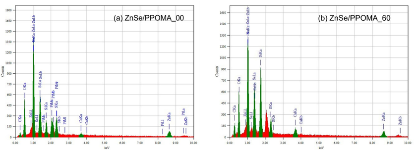
Representative EDX spectra of the hybrid thin films: (a) ZnSe/PPOMA_00 and (b) ZnSe/PPOMA_60.
Detected Elements
ZnSe/PPOMA_00
(at%)ZnSe/PPOMA_30
(at%)ZnSe/PPOMA_45
(at%)ZnSe/PPOMA_60
(at%)
C
17.63
24.39
37.10
37.18
O
35.88
29.20
23.19
21.08
N
−
3.12
5.02
7.31
Na
16.09
13.50
10.37
10.46
Si
3.89
2.69
9.09
6.80
S
5.69
4.32
2.85
2.89
Ca
0.72
0.74
1.14
1.17
Zn
12.25
13.56
6.77
6.71
Se
7.83
8.47
4.49
6.61
H
−
−
−
−
Total
100.00
100.00
100.00
100.00
3.3 X-ray diffraction analysis
XRD is an effective tool to identify crystallinity of the samples and the spectrum of ZnSe and ZnSe/PPOMA hybrid thin films with different amounts of PPOMA layers are shown in Fig. 4. It is apparent from the inset that there is no well-defined peak except a wide hump between 2θ values of 18° and 27°, indicating that the structure of the PPOMA thin films is amorphous in nature. However, the XRD spectra of ZnSe are well recognized as polycrystalline and have a cubic (zinc blende) structure. The diffraction peaks are labeled with their corresponding Miller indices (hkl). In all the samples, a prominent peak is observed at approximately (2θ = ) 32°, which corresponds to an inter-planar spacing of about 2.78 Å, indicating the presence of (1 1 1) reflections planes, which is a characteristic peak of the cubic zinc blende structure (Rusu et al., 2007). This observation suggests that the film crystallites are primarily aligned with their (1 1 1) planes parallel to the substrate. With the increase of PP deposition time of PPOMA, an increase of peak intensities of (1 1 1) plane of the hybrid films occurred indicating the improvement in the film structure. Zn and Se metal peaks appear in the XRD spectra (Indirajith et al., 2014). The tiny amount of Se metal throughout the co-reduction of Zn and Se might be due to the heterogeneous reaction among Zn2+ and Se2− in an acidic medium (Kumar et al., 2018) and the ZnO appeared in the joint often organic–inorganic layer owing to oxidation (Kamal and Science, 2011).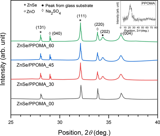
XRD spectra of ZnSe/PPOMA hybrid thin films with PPOMA film deposited onto ZnSe films for different durations (inset: PPOMA film).
The crystallite size (D) of the hybrid thin films has been determined using the Debye-Scherrer formula (Cullity, 1956), which relies on the full width at half maximum (β) of the peaks expressed in radians,
Where λ denotes the wavelength of CuKα radiation (1.54178 Å), K is the Scherrer constant (K = 0.90),
expresses the Bragg angle. The relationships provided below were employed to assess the microstrain (ε), dislocation density (δ), micro-stress (σstress) and lattice constant (a),
Where d′ is the interplanar spacing calculated from Brag's laws, h, k, l are the lattice planes, and E is the standard Young's modulus of the films material (ZnSe), 70.3 GPa (Ma et al., 2019). The structural parameters for the (1 1 1) plane, including D, ε, σstress and a, have been calculated and are presented in Table 2.
Sample ID
Crystallite size,
D (nm)Micro strain, ε
Micro stress, σstress
(10−2 Gpa)Lattice constant,
a (Å)
ZnSe/PPOMA_00
40.41 ± 4
0.0050
0.1773
4.797 ± 0.5
ZnSe/PPOMA_30
42.30 ± 3
0.0043
0.1516
4.796 ± 0.4
ZnSe/PPOMA_45
43.29 ± 3
0.0035
0.1244
4.747 ± 0.6
ZnSe/PPOMA_60
45.37 ± 5
0.0034
0.1228
4.797 ± 0.6
The typical D values are observed to vary with the thickness of the deposited PPOMA layer onto ZnSe thin films. Maximum average D for ZnSe/PPOMA_60 samples is 45.37 nm, while minimum average D for ZnSe/PPOMA_00 samples is 40.41 nm. The increase of the average D probably causes surface smoothness with PPOMA deposition time, which is supported by the result of the FESEM study. On the other hand, δ value decreases in the hybrid film, which indicates an improvement in the crystal structure and a reduction in defects or disruptions in the crystal lattice. Moreover, the relatively low value of ε also indicates a more ordered crystal structure. However, the a remains relatively constant for all the samples. This implies that the crystal structure of the ZnSe is almost independent of the PPOMA film thickness in ZnSe thin films.
3.4 Thermal analyses
TG and DSC are two commonly used techniques to study the thermal stability and decomposition behavior of the material. For the hybrid films produced by CBD and plasma polymerization techniques, the experiments were carried out in N2 environment with a heating rate of 10 °C/min over a temperature range of 27 to 600 °C. The weight losses of ZnSe/PPOMA thin films can be divided in different temperature regions as shown in Fig. 5(a). Table 3 provides the weight losses in the regions A, B, C and D for the as-deposited hybrid thin films.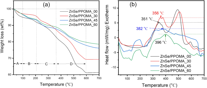
(a) TGA thermograms, (b) DSC of ZnSe/PPOMA hybrid films under N2 atmosphere at a scanning rate of 10 °C/min.
Region
Temperature (°C)
Weight loss (%)
ZnSe/PPOMA_00
ZnSe/PPOMA_30
ZnSe/PPOMA_45
ZnSe/PPOMA_60
A
27 − 100
5.10
3.00
3.30
3.30
B
100 − 207
8.14
4.47
6.83
6.46
C
207 − 360
17.00
12.68
12.21
11.04
D
360 − 600
32.40
30.58
22.18
20.20
Stability temperature
351 °C
356 °C
382 °C
396 °C
In region A (27 to 100 °C) the weight losses are relatively low and decrease with increasing PPOMA deposition time. Specifically, the weight losses recorded for all the films are within ∼ 5 %. This suggests that ZnSe/PPOMA films are more thermally stable in this temperature region, and the weight loss is likely due to the evaporation of small molecular mass species like CO2 and H2O (Park et al., 2018). In region B (100 − 207 °C) weight loss varies from 4.47 to 8.14 wt% for the deposited films, and it may occur due to the removal of some loosely unreacted molecules or distinct to any changes in the ZnSe/PPOMA structure.
In regions C and D, a significant weight loss occurred, which could be due to thermal degradation or a breakdown of the deposited films. The percentages of maximum thermal decomposition in region D occurred for pure ZnSe film (∼32.40 %) and decreased with the increase of the PPOMA layer onto it, which is because different units in the hybrid structure may be difficult for molecules to be separated during the thermal degradation. This is because the different units of ZnSe and PPOMA may have different thermal stabilities, and the weaker ZnSe unit may degrade first while the stronger unit remains intact. Therefore, it can be said that the presence of PPOMA films on ZnSe may increase the thermal stability of the hybrid film (Ning et al., 2017; Filipović et al., 1992).
The DSC thermogram in Fig. 5 (b) shows an exothermic wide band with peaks at different temperatures for ZnSe/PPOMA hybrid films. The stability temperatures are observed to be at 351, 356, 382, and 396 °C for the samples ZnSe/PPOMA_00, ZnSe/PPOMA_30, ZnSe/PPOMA_45 and ZnSe/PPOMA_60, respectively. After this temperature, an endothermic reaction is started owing to the thermal breakdown in the polymer chains. However, it is noted that the ZnSe/PPOMA_60 film is thermally more stable. It can be conjectured that owing to the stronger crosslinking among the PPOMA layer the hybrid films are more thermally stable compared to the pure ZnSe (ZnSe/PPOMA_00) film, which also depends on the thickness of the organic layer onto it (Sheikh et al., 2023).
3.5 Optical properties
The optical properties of the ZnSe/PPOMA hybrid thin films were examined in the wavelength range of 300 to 700 nm at room temperature. The variation in absorbance, A, of the hybrid films as a function is depicted in Fig. 6(a). It is observed that the ZnSe film showed the minimum A, which increases with the increase of thickness of the hybrid films. It may be due to either an increase in scattering or an increase in carbon content in the hybrid films observed in the EDX analysis. Due to the presence of the π–π* conjugation, the peak values of A for all the samples are located in the lower region (<400 nm) (Bayram and Simsek, 2018). The peak A of the hybrid films occurs in the lower than that of the ZnSe thin film. It means a blue shift occurred in the hybrid film owing to the increase in conjugate bond length during the hybrid film formation, which would be responsible for the change in the optical band gap (Xu et al., 2018; Wadatkar and Waghuley, 2022).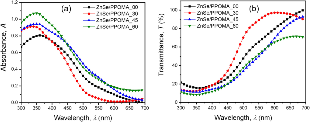
Spectral distribution of (a) absorbance and (b) transmittance as a function of wavelength for the ZnSe/PPOMA films.
The optical transmittance T of the ZnSe/PPOMA hybrid films as shown in Fig. 6(b) lifts with λ at the lower visible region (360 – 600 nm) and becomes almost saturated with T values of 75 to 90 % in the higher λ region (600 – 700 nm). The hybrid films have lower transmittance compared to pure ZnSe films, because of the PPOMA layer formed on the top of the films. However, the overall transmittance properties in the visible region of these films are quite linear compared to earlier ZnSe films studied by other researchers (Mehta et al., 2009; Ali et al., 2006).
The absorption coefficient (α) in Fig. 7(a) of the hybrid thin films was calculated using Eq. (7), with the help of A and the film thickness, d.
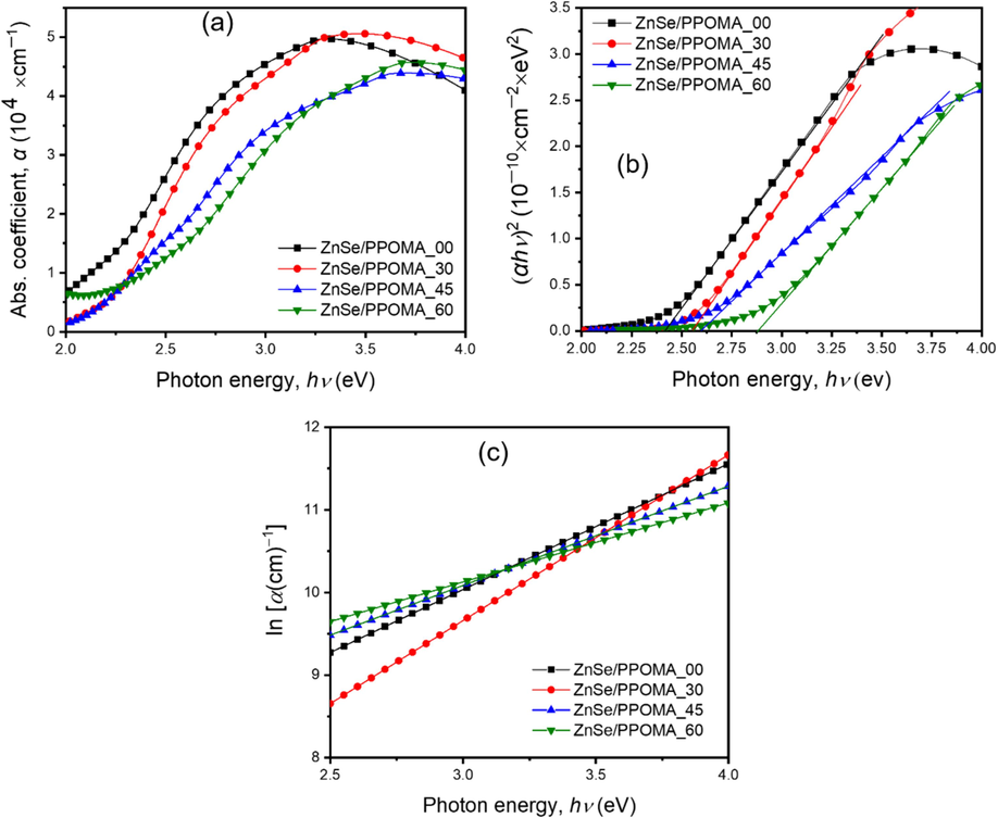
(a) Absorption coefficient, α, (b) direct band gap, Eg, and (b) lnα versus hν plots for the ZnSe/PPOMA thin films.
The less light enters the substrate before being absorbed the higher the absorption rate. For all ZnSe/PPOMA thin films α rises with increasing hν in the range of 2.0 to 3.4 eV and then sharply decreases between 3.5 eV and 4.6 eV. In this study, the organic PPOMA layer was deposited onto the inorganic ZnSe layer creating a non–polymer–polymer complex interface of two different layers (Kamal and Science, 2011; Shirsath et al., 2020). There are some possibilities of the presence of irregularities in the interface owing to an inhomogeneous interface, which may cause more amorphous nature in the hybrid thin film (Zhang and Lin, 2011). Thus, the change in the physical structure of those films would cause less absorption coefficient and consequently higher optical band gaps.
The optical band gap, Eg, is related to the electronic structure of the material, which provides insights into the materials behavior in response to radiation, suggesting potential applications in electronic and photonic devices. The permitted Eg of the ZnSe/PPOMA thin films are evaluated using the well-known Tauc relation (Eq. (8).
Where the Tauc parameter C denotes the proportionality factor, and the index n denotes the type of optical transition. When n = ½, the intercept of the linear portion of (αhν)2 versus hv curve as shown in Fig. 7(b), represents the direct bandgap, Eg. The estimated values of Eg are shown in Table 4. Eg of the ZnSe/PPOMA is observed to be 2.4 eV, which increases with the increase of PPOMA deposition time (increased thickness of the organic layer). It can be estimated that as the dielectric layer in the hybrid film decreases the band gap increases. The interaction in the interface of the two different film components also causes the variation of the band gap. This complex interface may not be homogeneous and therefore, there are some possibilities of presence of irregularities in the interface, which may cause more amorphous structure of the hybrid thin film. It should be noted that in most inhomogeneous/amorphous polymeric systems, the electronic conductivity is affected by this interface. The crosslinking between the interfaces should also be taken into consideration in this system, which may cause less absorption coefficient and consequently higher optical band gaps with increasing the PPOMA layer thickness. However, The dissimilarity of Eg suggests an idea of tuning the flexible optical band gap by changing the organic layer in hybrid films, which are desired for various sensing and optoelectronics applications.
Sample ID
Thickness, d (nm)
Maximum wavelength λmax (nm)
Eg (eV)
Urbach energy, EU (eV)
ZnSe/PPOMA_00
373 ± 7
360.28
2.4
0.94
ZnSe/PPOMA_30
415 ± 3
339.31
2.5
0.83
ZnSe/PPOMA_45
494 ± 5
348.70
2.6
0.79
ZnSe/PPOMA_60
540 ± 4
347.88
2.8
0.66
The Urbach energy (EU), which indicates the presence of disorder or defect states in the optical band gap region, also proves the dissimilarities of Eg. Eq. (9) (Hassanien et al., 2023) was used to calculate the values of Eu in the nonlinear portion of the optical band gap spectrum and presented in Table 4.
where E is the energy of the incident photon and α0 is a constant. The inverse gradient of the lnα versus hν plots as shown in Fig. 7 (c) directly specifies the Urbach energy. It is observed that the value of EU for pure ZnSe thin film is 0.94 eV and EU varies from 0.83 to 0.65 eV for the hybrid thin film. It can be conjectured that the percolation of two layers with each other may create an obstacle to forming Urbach tails between the localized state between the valance and conduction band of the hybrid film, which reduces the value of Urbach energy, and consequently, the optical band gap increases (Hassanien et al., 2020). The optical band gap of ZnSe/PPOMA hybrid film exhibits a notable dependency on the extent of PPOMA layer. The variations in elemental composition, structural configuration, and optical properties observed in the transition from pure ZnSe to hybrid films are significant, also emerges as a promising alternative material to traditional pure materials.
4 Conclusions
ZnSe/PPOMA hybrid thin films have been successfully fabricated through a two-step deposition process, which involved a chemical bath technique to create the inorganic layer of ZnSe, and a capacitively coupled plasma polymerization method to deposit the organic PPOMA layer. Here, heat-treated ZnSe film is taken as the base material on which the PPOMA layer is deposited with varying deposition times. The ZnSe/PPOMA film thickness is controlled by the deposition time of PPOMA and is found to increase from 373 to 540 nm. Hybrid films showed improved surface morphology with pinhole-free smooth surfaces as compared to inorganic ZnSe films, which is confirmed by FESEM analysis. This is due to the incorporation of two different layers and high crosslinking properties of PPOMA film. The energy-dispersive X-ray replicates the elemental compositions of the deposited hybrid films while X-ray diffraction analysis reveals the commendable crystallinity of the film. The as-deposited hybrid films are thermally stable up to 396 °C, which is considerably higher than other ZnSe films studied by different researchers. The value of Eg of the pure ZnSe (ZnSe/PPOMA_00) film is observed to be 2.54 eV and increases from 2.5 to 2.8 eV with the increase of PPOMA coating layer in the ZnSe/PPOMA films. Other optical parameters such as absorbance, transmittance, absorption coefficient and Urbach energy are varied accordingly. These results highlight the potential of these bilayer hybrid thin films for a wide range of applications, particularly in the realm of passive thin films for use in cutting-edge sensing, optical devices, and buffer layers in solar cell fabrication entirely free of Cd.
CRediT authorship contribution statement
Farzana Yasmin: Conceptualization, Data curation, Formal analysis, Investigation, Methodology, Writing – original draft, Writing – review & editing. Md. Saddam Sheikh: Formal analysis, Investigation, Validation, Visualization, Writing – original draft, Writing – review & editing. A.H. Bhuiyan: Validation, Visualization, Writing – review & editing. Mohammad Jellur Rahman: Conceptualization, Supervision, Validation, Visualization, Writing – review & editing.
Acknowledgments
The authors express their gratitude to the Committee for Advanced Studies and Research of Bangladesh University of Engineering and Technology for the financial assistance. Additionally, they appreciate the support from the Nanotechnology Research Laboratory of the Department of Physics at BUET, which facilitated access to UV-visible spectra. The authors also extend their gratitude to the Bangladesh Council of Scientific and Industrial Research for their essential support in recording FESEM-EDX data.
Declaration of Competing Interest
The authors declare that they have no known competing financial interests or personal relationships that could have appeared to influence the work reported in this paper.
References
- Carrier transport mechanisms of iodine-doped plasma polymerised N, N, 3, 5 tetramethylaniline thin films. Mater. Today Commun.. 2022;31:103377
- [CrossRef] [Google Scholar]
- Insights into the structural and optical features of plasma polymerized N, N, 3, 5 tetramethylaniline-2,6-diethylaniline thin films. Opt. Mater.. 2023;144:114278
- [CrossRef] [Google Scholar]
- Physical properties of ZnSe films prepared by two-source evaporation and a study of post doping effect. J. Non. Cryst. Solids.. 2006;352(5):409-414.
- [CrossRef] [Google Scholar]
- Nonlinear characterization of conducting polymer and electrical study for application as solar cells and its antibacterial activity. Optik (stuttg).. 2016;127(13):5301-5309.
- [CrossRef] [Google Scholar]
- A Study on the Optical, Chemical and Dielectric Properties of PPCIN Thin Films Derived from Essential Oil Compounds Using RF Plasma Polymerisation Technique.. 2018;156:198-204.
- [CrossRef]
- Optical and structural characterization of ZnSe thin film fabricated by thermal vapour deposition technique. AIMS Mater. Sci.. 2017;4(5):1095-1121.
- [CrossRef] [Google Scholar]
- Chowdhury, M. T., M., Zubair, A. H. Takeda, Hussain, K. M. A. and Islam, M. F., 2017. Optical and structural characterization of ZnSe thin film fabricated by thermal vapour deposition technique. AIMS Mater. Sci., vol. 4, pp. 1095–1121. doi: 10.3934/matersci.2017.5.1095.
- Elements of X-ray Diffraction. Addison-Wesley Publishing; 1956.
- Effect of deposition temperature on structural and optical properties of chemically grown nanocrystalline Ni doped ZnS thin films. J. Alloys Compd.. 2016;658:780-787.
- [CrossRef] [Google Scholar]
- Study of the isothermal bulk polymerization of dimethyl phenyl methacrylates by differential scanning calorimetry. Thermochim. Acta.. 1992;205(C):139-144.
- [CrossRef] [Google Scholar]
- Study of optical properties of thermally evaporated ZnSe thin films annealed at different pulsed laser powers. J. Alloys Compd.. 2016;685:733-742.
- [CrossRef] [Google Scholar]
- Physical and optical studies of the novel non-crystalline CuxGe20-xSe40Te40 bulk glasses and thin films. J. Alloys Compd.. 2020;849:156718
- [CrossRef] [Google Scholar]
- Inference of Sn addition on optical properties of the novel thermally evaporated thin a-Ge15Te50S35-xSnx films and some physical properties of their glasses. Mater. Chem. Phys.. 2023;293:126887
- [CrossRef] [Google Scholar]
- The effect of annealing time on zinc selenide thin films deposited by photo-assisted chemical bath deposition. J. Phys. Chem. Solids.. 2020;140:109381
- [CrossRef] [Google Scholar]
- Synthesis of ZnSe nano particles, deposition of ZnSe thin films by electron beam evaporation and their characterization. Ferroelectrics. 2014;467(1):13-21.
- [CrossRef] [Google Scholar]
- High-responsivity solution-processed organic-inorganic hybrid bilayer thin film photoconductors. J. Mater. Chem. C. 2013;1(48):7996-8002.
- [CrossRef] [Google Scholar]
- Low-voltage-operating complementary-like circuits using ambipolar organic-inorganic hybrid thin-film transistors with solid-state-electrolyte gate insulator. Org. Electron.. 2019;75:105358
- [CrossRef] [Google Scholar]
- Kamal, M., Science, A. B.-J. of A. P., 2011. Optical characterization of plasma‐polymerized pyrrole‐N,N,3,5‐tetramethylaniline bilayer thin films. Wiley Online Libr. 121(4), 2361–2368. doi:10.1002/app.33176.
- Paper based organic–inorganic hybrid photodetector for visible light detection. Appl. Surf. Sci.. 2020;524:146589
- [CrossRef] [Google Scholar]
- Optical and structural properties of CdSe thin film produced by chemical bath deposition. J. Non-Oxide Glas.. 2016;8(1):1-9.
- [Google Scholar]
- Comparative study of structural, optical and electrical properties of electrochemically deposited Eu, Sm and Gd doped ZnSe thin films. J. Mater. Sci. Mater. Electron.. 2018;29(7):5638-5648.
- [CrossRef] [Google Scholar]
- Kumar P, S., Jayanarayanan, K., Balachandran, M., 2023. High-performance thermoplastic polyaryletherketone/carbon fiber composites: Comparison of plasma, carbon nanotubes/graphene nano-anchoring, surface oxidation techniques for enhanced interface adhesion and properties. Compos. Part B Eng. 253, 110560. doi:10.1016/J.COMPOSITESB.2023.110560.
- Review of Organic/Inorganic Thin Film Encapsulation by Atomic Layer Deposition for a Flexible OLED Display. JOM.. 2019;71(1):197-211.
- [CrossRef] [Google Scholar]
- Molecular layer deposition of indicone and organic-inorganic hybrid thin films as flexible transparent conductor. Appl. Surf. Sci.. 2020;525:146383
- [CrossRef] [Google Scholar]
- Organic-Inorganic Hybrid Thin Films Fabricated by Layer-by-Layer Assembly of the Phosphorylated Cellulose Nanocrystal and Imogolite Nanotubes. Langmuir.. 2018;34(44):13361-13367.
- [CrossRef] [Google Scholar]
- Reinforcing carbon fiber epoxy composites with triazine derivatives functionalized graphene oxide modified sizing agent. Compos. Part B Eng.. 2019;176:107078
- [CrossRef] [Google Scholar]
- Effect of deposition parameters on structural, optical and electrical properties of nanocrystalline ZnSe thin films. Appl. Surf. Sci.. 2009;256(3):608-614.
- [CrossRef] [Google Scholar]
- Muntaz B., S., Ravindranadh, K., Ravikumar, R. V. S. S. N., Rao, M. C. 2016. Structural and luminescent properties of PVA capped ZnSe nanoparticles. Mater. Res. Innov. 22, 37–42. doi: 10.1080/14328917.2016.1265254.
- Preparation and characterization of zinc oxide/TEMPO-oxidized cellulose nanofibril composite films. Cellulose.. 2017;24(11):4861-4870.
- [CrossRef] [Google Scholar]
- Review of Materials and Fabrication Methods for Flexible Nano and Micro-Scale Physical and Chemical Property Sensors. Appl. Sci.. 2021;11(18):8563.
- [CrossRef] [Google Scholar]
- Thermal Analysis on the Stabilization Behavior of Ternary Copolymers Based on Acrylonitrile, Methyl Acrylate and Itaconic Acid. Fibers Polym.. 2018;19(12):2439-2448.
- [CrossRef] [Google Scholar]
- Structural and optical properties of plasma polymerized o-methoxyaniline thin films. Thin Solid Films.. 2013;534:132-136.
- [CrossRef] [Google Scholar]
- Enhanced UV photodetector performance in bi-layer TiO2/WO3 sputtered films. Appl. Surf. Sci.. 2019;494:575-582.
- [CrossRef] [Google Scholar]
- Structural characterization and optical properties of ZnSe thin films. Appl. Surf. Sci.. 2007;253(24):9500-9505.
- [CrossRef] [Google Scholar]
- Reducing crystallinity on thin film based CMC/PVA hybrid polymer for application as a host in polymer electrolytes. J. Non. Cryst. Solids.. 2019;511:201-211.
- [CrossRef] [Google Scholar]
- Nanocrystalline ZnSe thin films prepared by solution growth technique for photosensor application. Compos. Part B Eng.. 2013;44(1):553-557.
- [CrossRef] [Google Scholar]
- Thickness dependence of structural and optical behavior of plasma polymerized 3, 4-ethylenedioxythiophene thin films. Opt. Mater.. 2022;134(PA):113170
- [CrossRef] [Google Scholar]
- Direct current conduction mechanism in the methyl acrylate – vinyl acetate composite thin films. Sci. Rep.. 2023;1–11
- [CrossRef] [Google Scholar]
- Structural and optical behaviours of methyl acrylate-vinyl acetate composite thin films synthesized under dynamic low-pressure plasma. Heliyon.. 2023;9(8)
- [CrossRef] [Google Scholar]
- Interface-Charge Induced Giant Electrocaloric Effect in Lead Free Ferroelectric Thin-Film Bilayers. Nano Lett.. 2020;20(2):1262-1271.
- [CrossRef] [Google Scholar]
- Chemical Bath Deposition of ZnSe Thin Films: Investigations of the Growth Conditions. Am. Chem. Sci. J.. 2016;14(4):1-6.
- [CrossRef] [Google Scholar]
- Effect of pH on the structural and optical properties of polycrystalline ZnSe thin films produced by CBD method. Int. J. Mod. Phys. B. 2019;33(5):1-13.
- [CrossRef] [Google Scholar]
- A study of structural, morphological, optical and electrical properties of Zinc Selenide (ZnSe) thin film. Mater. Today Proc.. 2016;3(6):2305-2314.
- [CrossRef] [Google Scholar]
- Mehrfachreflex-Interferometrie an Oberflächen und Schichten. Phys. J.. 1948;4(11–12):472-480.
- [CrossRef] [Google Scholar]
- Effect of RF power on the physical properties of sputtered ZnSe nanostructured thin films for photovoltaic applications. Nanomaterials. 2021;11(11):1-15.
- [CrossRef] [Google Scholar]
- Synthesis and Complex Optical Characterization of Polythiophene/Poly (vinyl acetate) Composite Thin Films for Optoelectronic Device Applications. Pure Appl. Phys.. 2022;60(5):430-436.
- [Google Scholar]
- Organic/inorganic hybrid sensors: A review. Sensors Actuators, B Chem.. 2013;182:467-481.
- [CrossRef] [Google Scholar]
- Investigation on the structure and optical properties of chemically deposited ZnSe nanocrystalline thin films. Phys. Condens. Matter.. 2013;410:120-125.
- [CrossRef] [Google Scholar]
- Tuning band gap, color switching, optical contrast, and redox stability in solution-processable BDT-based electrochromic materials. Org. Electron.. 2018;54:94-103.
- [CrossRef] [Google Scholar]
- Enhanced light extraction from organic light-emitting devices through non-covalent or covalent polyimide–silica light scattering hybrid films. J. Mater. Chem. c.. 2020;8:4102-4111.
- [CrossRef] [Google Scholar]
- Organic–inorganic hybrid thin film light-emitting devices: interfacial engineering and device physics. J. Mater. Chem. c.. 2021;9(5):1484-1519.
- [CrossRef] [Google Scholar]
- Zhang, W., Lin, C. Te; Liu, K. K., Tite, T., Su, C. Y., Chang, C. H., 2011. Opening an electrical band gap of bilayer graphene with molecular doping. ACS Nano. 5(9), 7517–7524. doi:10.1021/NN202463G/SUPPL_FILE/NN202463G_SI_001.PDF.