

Translate this page into:
An indirect-to-direct band gap transition of NaSbS2 via minor Ga doping: A theoretical study
⁎Corresponding authors. rjsa@mju.edu.cn (Rongjian Sa), liudiwen1987@163.com (Diwen Liu)
-
Received: ,
Accepted: ,
This article was originally published by Elsevier and was migrated to Scientific Scholar after the change of Publisher.
Peer review under responsibility of King Saud University.
Abstract
The efficiency of NaSbS2 is limited by its wide indirect band gap. Alloying is a very effective strategy to tune the band gap over a wide range for the mixed-anion NaSb(S,Se)2 alloys. However, these compounds are still indirect band gap semiconductors. The influence of Ga doping on the structure, electronic, and optical properties of NaSbS2 is studied for the first time. Our calculated results show that NaSbS2 is an indirect band gap semiconductor, and the difference between the indirect and direct band gaps is less than 0.1 eV. Moreover, the forbidden transition is discovered for the fundamental direct bandgap of NaSbS2. The results indicate that the NaSb1-xGaxS2 alloys are predicted to be synthesized in the proper conditions. An indirect-to-direct band gap transition is observed from NaSbS2 to NaSb1-xGaxS2. The minor Ga doping (less than10 %) has little effect on the electronic and optical properties of NaSbS2. Importantly, the weak transition of the fundamental direct bandgap is allowed for NaSb1-xGaxS2. This study can provide a route to explore the high efficiency of novel based-NaSbS2 materials.
Keywords
NaSbS2
Ga doping
Bandgap transition
Optical property

1 Introduction
Ternary metal chalcogenides with the formula of ABX2 (A = Na, K, Cu, Ag; B = Sb, Bi; and X = S or Se) have attracted considerable interest because of their huge potential applications in photovoltaics. These compounds are non-toxic or less toxic, earth abundant, and inexpensive. The experimental band gaps of NaBiS2 and NaBiSe2 are in the ideal range (1.20–1.45 eV) and they show great of interest for applications in solar cells (Rosales et al., 2018). KBiS2 and KBiSe2 exhibit remarkable stability and strong optical absorption in the whole visible range.(Yang et al., 2019) The structure and optoelectronic properties of ternary metal chalcogenides CuSb(S,Se)2 (Choi et al., 2015; Welch et al., 2015) and Ag(Sb,Bi)S2 (Ho and Lee, 2013; Huang et al., 2013) have been studied in the past few years as the potential alternatives for applications in solar cells. High-throughput calculations for screening potential photovoltaic absorbers have been performed by computing the band gap and effective mass of carriers and 31 candidates are identified (Kang et al., 2019). Finally, taking earth abundance and low cost into account, three compounds GeAs2, SiAs2, and NaSbS2 are considered as promising indirect bandgap semiconductors. In addition, the defect properties are studied in order to provide a guideline for optimizing growth conditions of these materials.
NaSbS2 is a kind of compound with the excellent properties of non-toxic, earth-abundant, and good stability. NaSbS2 shows an optical band gap of 1.5–1.8 eV and high absorption coefficient (Bazakutsa et al., 1975; Rahayu et al., 2016). The initial efficiency of 3.18 % was achieved in 2016 for the first time (Rahayu et al., 2016). In 2018, the higher efficiency was 4.11 % for NaSbS2. The structural, thermoelectric, electronic, and optical properties of NaSbS2 and NaSbSe2 have been investigated by using first-principles method (Dai et al., 2019; Khare et al., 2020; Mahmoud et al., 2019; Sun and Singh, 2017; Zhang et al., 2019). The recent theoretical study indicates that NaSbS2 might be limited for solar cells due to the forbidden transition of fundamental direct bandgap (Leung et al., 2019). NaSbSe2 has a narrower band gap of 1.48 eV and yields an efficiency of 2.22 % (Aragaw et al., 2017). The efficiency can be further improved by tuning the band gap of NaSbS2 to the optimal bandgap (∼1.4 eV) through adjusting the NaSb(S,Se)2 alloy composition (Dai et al., 2019). Recently, the structural, mechanical, electronic, and optical properties of Na1-xLixSbS2 solid solutions have been performed (Liu et al., 2021). The results show that the suitable band gap of NaSbS2 can be achieved by doping Li and applying moderate pressure. In addition, NaSbX2 and NaInX2 (X = S or Se) belong to the hexagonal (space group: R-3 m) and monoclinic (space group: C2/c) crystal structures, respectively (Hoppe et al., 1961; Olivier-Fourcade et al., 1978). Therefore, the compound NaBX2 (X = S or Se) will undergo phase transition when Sb is replaced by In with a larger ion radius. The experimental and theoretical works have confirmed that NaInX2 has a broader band gap than that of NaSbX2 (Fukuzaki et al., 2000; Hossain et al., 2021b; Takahashi et al., 2018). The structural, elastic, and thermal properties of various NaInS2-xSex compounds have been explored in detail (Hossain et al., 2021a). Interestingly, three compounds KInS2, RbInS2, and CsInS2 show the monoclinic crystal structures with space group C2/c (Eisenmann and Hofmann, 1991; Zeng et al., 2007), and they have larger direct band gaps (Bouchenafa et al., 2018).
The crystal structure and optical band gap of NaGaS2 was studied by two research groups for the first time in 2020 (Adhikary et al., 2020; Klepov et al., 2020). NaGaS2 is a monoclinic crystal structure with the C2/c space group and shows a wide optical band gap (∼4.0 eV) (Adhikary et al., 2020). The recent theoretical calculations show that NaGaS2 is a direct band gap compound (Yun et al., 2022). Our calculated results suggest that NaSbS2 is a narrow indirect band gap semiconductor (Liu et al., 2021). Therefore, an indirect-to-direct band gap transition can be achieved from NaSbS2 to NaGaS2. Ga and Sb have similar ionic radii, so it is theoretically feasible to synthesize the NaSb1-xGaxS2 alloys. It should be pointed out that the doping Ga concentration must be controlled because high Ga doping concentration will lead to a significant increase in band gap of NaSbS2. Here, the influence of Ga doping on the structure, electronic and optical properties of NaSbS2 is reported based on first-principles calculations. It is discovered that the Ga minor doping is an effective strategy to obtain the direct band gap of highly stable NaSbS2. The low concentration Ga doping has little effect on the electronic and optical properties of NaSbS2. Moreover, the weak transition is allowed for the fundamental direct bandgap of NaSb1-xGaxS2. The present study can inspire experiment research to explore more novel based-NaSbS2 materials with high efficiency.
2 Computational details
All the calculations were carried out via density functional theory (DFT), which was implemented in Vienna ab initio simulation package (VASP) (Kresse and Furthmüller, 1996). The generalized gradient approximation of Perdew-Burke-Ernzerhof (GGA-PBE) (Perdew et al., 1996) was used to deal with the exchange–correlation effects. The interactions between ions and electrons were described by the projector-augmented wave (PAW) (Blöchl, 1994) method with an energy cutoff of 350 eV. The valence electron configurations for Na, Sb, Ga, and S were 2p63s1, 5s25p3, 4s24p1, and 3s23p4, respectively. The geometry optimization convergence criteria were set to 1.0 × 10⁻⁵ eV and 0.01 eV/Å for total energy and the force on each atom, respectively. A 6 × 6 × 6 k-point mesh was employed for NaSbS2 and NaSb0.75Ga0.25S2. 3 × 3 × 3, 6 × 3 × 3, and 6 × 6 × 3 k-point meshes were selected for NaSb1-xGaxS2 with three doping concentrations of × = 0.03125, 0.0625, and 0.125, respectively.
3 Results and discussions
3.1 Structural properties
The monoclinic phase with space group C2/c of NaSbS2 is chosen as the object of this study. The crystal structure of NaSbS2 is depicted in Fig. 1. The calculated lattice constants of NaSbS2 are a = 8.24 Å, b = 8.40 Å, and c = 6.91 Å, which are in good agreement with the experimental data (Olivier-Fourcade et al., 1978). In order to explore the impact of Ga doping on the physical properties of NaSbS2, different supercells are modeled. The doping concentration is related to supercell size. There are four formula units (16 atoms) for the pristine NaSbS2, so the NaSb0.75Ga0.25S2 compound is simulated by substituting one Ga atom for one Sb atom. Accordingly, the NaSb1-xGaxS2 (x = 0.03215, 0.0625, and 0.125) compounds are simulated by 2 × 2 × 2, 1 × 2 × 2, and 1 × 1 × 2 supercells when one Sb atom is replaced by one Ga atom. The local structural variation of NaSbS2 is caused by the introduction of Ga atoms. For instance, the bond length is significantly shortened from Sb − S to Ga − S due to the smaller ionic radius of Ga3+. According to our recent theoretical study (Sa et al., 2022), NaSbS2 exhibits high stability. The thermodynamic stability of compound can be evaluated by calculating the formation enthalpy (ΔH). The stability of NaSb1-xGaxS2 is assessed in the present work by the following equation:
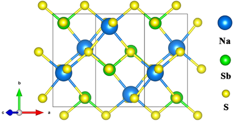
Crystal structure of NaSbS2.
where E(NaSb1-xGaxS2), E(NaSbS2), E(Sb) and E(Ga) refer to the total energies of compounds and the energies of solid state Sb and Ga atoms, respectively. The calculated ΔH value of NaSb1-xGaxS2 is displayed in Fig. 2. The negative ΔH value confirms the stability of NaSb1-xGaxS2. It can be seen that there is no difference in the stability of NaSbS2 with low concentration Ga doping. Moreover, the stability of NaSbS2 is slightly reduced when the concentration of Ga doping is high.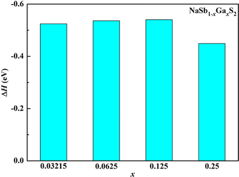
The formation energies of the NaSb1-xGaxS2 compounds.
3.2 Electronic structure
The band structure and density of states of NaSbS2 are analyzed, as shown in Fig. 3. The indirect band gap nature of NaSbS2 is observed because the valence band maximum (VBM) and conduction band minimum (CBM) are located at the high symmetry Z and τ points, respectively. Several theoretical reports suggest that NaSbS2 is an indirect band gap material (Kang et al., 2019; Mahmoud et al., 2019; Sun and Singh, 2017; Xia et al., 2017), while another theoretical study describes this compound to have a fundamental direct band gap (Leung et al., 2019). The indirect and direct band gaps are 0.88 and 0.98 eV for NaSbS2, which is much smaller than the previous experimental data (Leung et al., 2019; Rahayu et al., 2016). The energy difference between the indirect and direct band gaps is small (only 0.1 eV). It is well known that the GGA-PBE method usually underestimates the band gap of semiconductor material. More accurate band gap can be obtained for NaSbS2 from hybrid functional HSE06 (Liu et al., 2021). The band gap variation trend with various components from both PBE and HSE06 methods is similar (Fang et al., 2019). Therefore, the band gap underestimated by the DFT method has no effect on the trend of band gap variation of materials with various components. In addition, the HSE06 method is not suitable for calculating the band structure of NaSbS2 with minor Ga doping. The trend of band gap variation of NaSb1-xGaxS2 is predicted by the DFT method in the present study. In NaSbS2, the VBM is mainly dominated by the S-3p orbitals, while the CBM are contributed from the Sb-5p and S-3p orbitals. It is noted that Na has no contribution to the band edges. Moreover, the flat CBM and slope VBM indicate that the effective mass difference between electron and hole is significant, and NaSbS2 is actually a p-type semiconductor.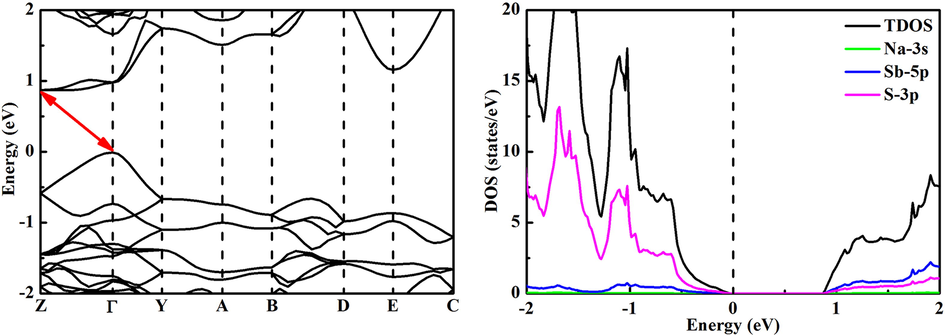
Band structure (left) and density of states (right) of NaSbS2.
Fig. 4 shows the band structure and density of states of NaSb1-xGaxS2 with different Ga concentrations. It can be seen from Fig. 4 that all the Ga-doped compounds are direct band gap semiconductors at the τ point. The results indicate that the transition from an indirect-to-direct band gap for NaSbS2 can be realized by doping Ga. The flat CBM and VBM imply that the large effective masses for electron and hole will exist, which is not preferred for thin-film solar cell applications. The contribution of the Ga-4 s and Ga-4p orbitals is negligible for the band edges when the doping Ga concentration is low. Therefore, it is speculated for NaSb1-xGaxS2 with × = 0.03125–0.125 that the small band gap variation may be caused by local structural changes. However, the CBM of NaSb0.75Ga0.25S2 is derived from the Sb-5p, Ga-4 s, and S-3p orbitals, and the VBM is still from the S-3p orbitals. It is clear that the intervention of the Ga-4 s orbitals is related to the larger bandgap of NaSb0.75Ga0.25S2. The band gap variation trend for NaSbS2 with various components is displayed in Fig. 5. An enlarged band gap is found for NaSbS2 when the doping Ga concentration increases. There is no obvious effect on the band gap of NaSbS2 when the doping Ga concentration is less than 10 %. The band gap increases by 0.5 eV from NaSbS2 to NaSb0.75Ga0.25S2. The results show that it is indeed an effective strategy to achieve the transition from an indirect to direct band gap for NaSbS2 with maintaining the initial electronic properties through the low concentration of Ga doping.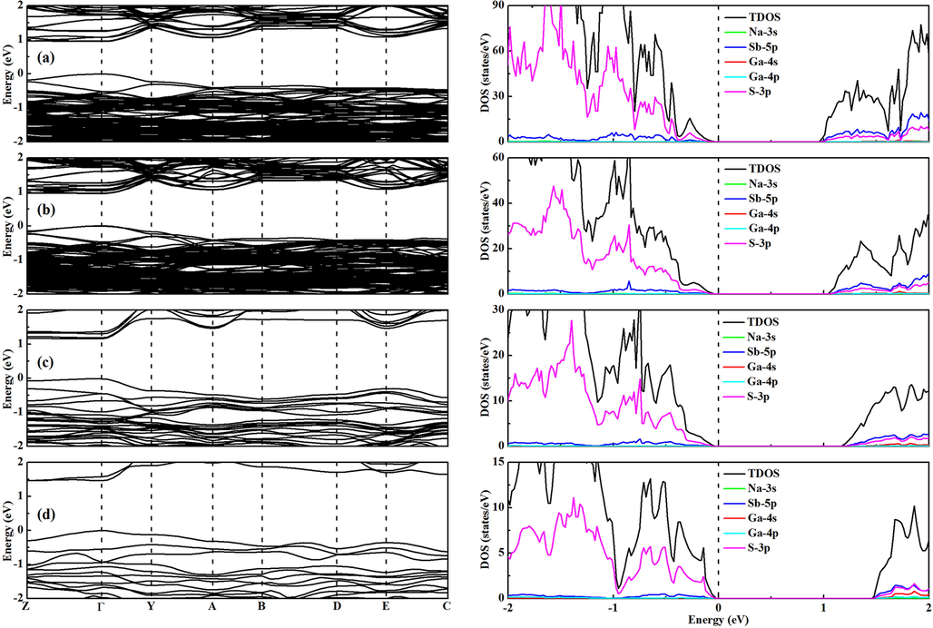
Band structure (left) and density of states (right) of NaSb1-xGaxS2 with different Ga concentrations: (a) 3.125%, (b) 6.25%, (c)12.5%, and (d) 25%.
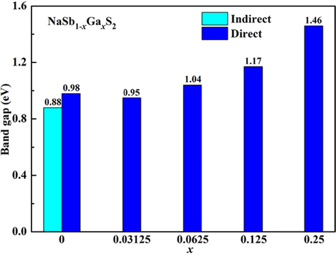
The band gap value of NaSb1-xGaxS2 as a function of Ga concentration.
The effect of parity-forbidden transition for halide perovskites was systematically reported in the previous theoretical study (Meng et al., 2017). For example, CsBI3 (B = Ge, Sn, Pb) with a direct band gap shows no parity-forbidden transitions at the R point. The transition probability between the VBM and CBM can be revealed by calculating the transition dipole moment (TDM). The computed TDM values of NaSbS2 and NaSb0.75Ga0.25S2 at various k points are shown in Fig. 6(a-b). It is clear that the calculated TDM value is zero at the τ point, which indicates that the transition is forbidden at the τ point. The direct allowed band gap of NaSbS2 at the Z point is 0.48 eV larger than the direct forbidden band gap at the τ point. It is observed from Fig. 6(b) that the transition is allowed at the τ point for NaSb0.75Ga0.25S2. Fig. 6(c) shows the calculated TDM value of NaSb1-xGaxS2 at the τ point as a function of Ga concentration. The results suggest that with the increase of low Ga content, the TDM value is small and increases slowly. The weak transition is allowed for NaSb1-xGaxS2 when it has a direct band gap at the τ point. The strong transition will be allowed for NaSb0.75Ga0.25S2 with a large TDM value. However, the band gap is greatly increased by doping high concentration of Ga. Therefore, the doping Ga concentration needs to be controlled reasonably for NaSbS2 in order to balance the values between TDM and band gap.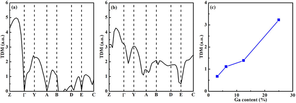
The TDM values of (a) NaSbS2 and (b) NaSb0.75Ga0.25S2 at various k points and (c) NaSb1-xGaxS2 at the τ point.
3.3 Optical properties
The optical properties α(ω) can be calculated by the real ε1(ω) and imaginary ε2(ω) parts of dielectric function ε(ω). Tωo parameters ε1(ω) and ε2(ω) are related to each other through Kramer-Kronig relation (Gajdoš et al., 2006). The calculated optical absorption spectra of NaSb1-xGaxS2 is presented in Fig. 7. The optical absorption is directly related to the band gap of the compound. The low concentration Ga-doped NaSbS2 and pure NaSbS2 show similar optical properties. The light absorption capacity of NaSb0.875Ga0.125S2 is slightly reduced compared to pure NaSbS2. The optical absorption coefficient of NaSb0.75Ga0.25S2 is lower than that of NaSbS2 in the range of 300–500 nm, which is attributed to the larger band gap. The relationship between the optical properties and bandgap is inversely proportional, and the decrease of optical absorption is mainly located near 400 nm. Therefore, it is expected to improve the photovoltaic performance of NaSbS2 with the help of the low concentration Ga doping.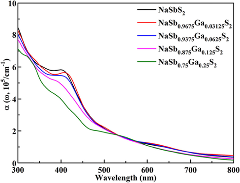
Computed optical absorption spectra of NaSb1-xGaxS2 with × = 0–0.25.
4 Conclusion
In summary, the present work is performed to discover the impact of Ga doping on the structure, electronic, and optical properties of NaSbS2. NaSbS2 is an indirect band gap compound, and the energy difference between the indirect and direct band gaps is small. The forbidden transition is found for the fundamental direct bandgap of NaSbS2. The negative ΔH values indicate that the NaSb1-xGaxS2 alloys can be synthesized and confirm their thermodynamic stability. An indirect-to-direct band gap transition is discovered from NaSbS2 to NaSb1-xGaxS2. The effect of low concentration Ga doping (less than10 %) is negligible for the electronic and optical properties of NaSbS2. However, the band gap of NaSbS2 is greatly increased when the concentration of Ga doping is high. Furthermore, the weak transition of the fundamental direct bandgap is allowed for NaSb1-xGaxS2. Therefore, this finding makes NaSbS2 more favorable for solar cells. Our study will contribute to improve the efficiency of based-NaSbS2 materials in the future.
Acknowledgments
This work was supported by the Open Project of Fujian Key Laboratory of Functional Marine Sensing Materials (No. MJUKF-FMSM202012).
Declaration of competing interest
The authors declare that they have no known competing financial interests or personal relationships that could have appeared to influence the work reported in this paper.
References
- Unusual atmospheric water trapping and water induced reversible restacking of 2D Gallium Sulfide layers in NaGaS2 formed by supertetrahedral building unit. Chem. Mater.. 2020;32:5589-5603.
- [Google Scholar]
- Ion exchange-prepared NaSbSe2 nanocrystals: electronic structure and photovoltaic properties of a new solar absorber material. RSC Adv.. 2017;7:45470-45477.
- [Google Scholar]
- Photoelectric and optical properties of thin films of ternary chalcogenides of the form MeISbX2VI. Sov. Phys. J.. 1975;18:472-475.
- [Google Scholar]
- Theoretical investigation of the structural, elastic, electronic and optical properties of the ternary indium sulfide layered structures AInS2 (A = K, Rb and Cs) Solid State Sci.. 2018;76:74-84.
- [Google Scholar]
- CuSbS2-sensitized inorganic-organic heterojunction solar cells fabricated using a metal-Thiourea complex solution. Angew. Chem. Int. Ed.. 2015;54:4005-4009.
- [Google Scholar]
- NaSbSe2 as a promising light-absorber semiconductor in solar cells: first-principles insights. APL Mater.. 2019;7:081122
- [Google Scholar]
- Crystal structure of potassium phyllo-dithioindate(III), KInS2. Z Krist. Cryst. Mater.. 1991;195:318-319.
- [Google Scholar]
- Bandgap alignment of α-CsPbI3 perovskites with synergistically enhanced stability and optical performance via B-site minor doping. Nano Energy. 2019;61:389-396.
- [Google Scholar]
- Preparation and characterization of NaInO2 and NaInS2. J. Mater. Chem.. 2000;10:779-782.
- [Google Scholar]
- Linear optical properties in the projector-augmented wave methodology. Phys. Rev. B. 2006;73:045112
- [Google Scholar]
- Influence of Se doping on recently synthesized NaInS2-xSex solid solutions for potential thermo-mechanical applications studied via first-principles method. Mater. Today Commun.. 2021;26:101988
- [Google Scholar]
- NaInX2 (X = S, Se) layered materials for energy harvesting applications: first-principles insights into optoelectronic and thermoelectric properties. J. Mater. Sci.: Mater. Electron.. 2021;32:3878-3893.
- [Google Scholar]
- AgBiS2 semiconductor-sensitized solar cells. J. Phys. Chem. C. 2013;117:18308-18314.
- [Google Scholar]
- Computational screening of indirect-gap semiconductors for potential photovoltaic absorbers. Chem. Mater.. 2019;31:4072-4080.
- [Google Scholar]
- Electronic, optical, and thermoelectric properties of sodium pnictogen chalcogenides: a first principles study. Comput. Mater. Sci.. 2020;183:109818
- [Google Scholar]
- NaGaS2: an elusive layered compound with dynamic water absorption and wide-ranging ion-exchange properties. Angew. Chem. Int. Ed.. 2020;59:10836-10841.
- [Google Scholar]
- Efficiency of ab-initio total energy calculations for metals and semiconductors using a plane-wave basis set. Comput. Mater. Sci.. 1996;6:15-50.
- [Google Scholar]
- An experimental and theoretical study into NaSbS2 as an emerging solar absorber. J. Mater. Chem. C. 2019;7:2059-2067.
- [Google Scholar]
- (Li, Na)SbS2 as a promising solar absorber material: a theoretical investigation. Spectrochim. Acta. A Mol Biomol. Spectrosc.. 2021;250:119389
- [Google Scholar]
- Structural, stability and thermoelectric properties for the monoclinic phase of NaSbS2 and NaSbSe2: a theoretical investigation. Eur. Phys. J. B. 2019;92:214.
- [Google Scholar]
- Parity-forbidden transitions and their impact on the optical absorption properties of lead-free metal halide perovskites and double perovskites. J. Phys. Chem. Lett.. 2017;8:2999-3007.
- [Google Scholar]
- Structure des composés NaSbS2α et NaSbS2β. Etude de l'influence de la paire electronique E de I'antimonine III dans Ia transition NaSbS2α → NaSbS2β. Z. Anorg. Allg. Chem.. 1978;446:159-168.
- [Google Scholar]
- Generalized gradient approximation made simple. Phys. Rev. Lett.. 1996;77:3865-3868.
- [Google Scholar]
- Sodium antimony sulfide (NaSbS2): Turning an unexpected impurity into a promising, environmentally friendly novel solar absorber material. APL Mater.. 2016;4:116103
- [Google Scholar]
- Solution-grown sodium bismuth dichalcogenides: toward earth-abundant, biocompatible semiconductors. J. Am. Chem. Soc.. 2018;140:3736-3742.
- [Google Scholar]
- Bandgap engineering of Na1-xAgxSbS2 alloys for photovoltaic applications. Mater. Res. Bull.. 2022;152:111862
- [Google Scholar]
- Electronic properties, screening, and efficient carrier transport in NaSbS2. Phys. Rev. Applied. 2017;7:024015
- [Google Scholar]
- Synthesis, crystal structure and optical absorption of NaInS2-xSex. J. Alloys Compd.. 2018;750:409-413.
- [Google Scholar]
- CuSbSe2 photovoltaic devices with 3% efficiency. Appl. Phys. Express. 2015;8:082301
- [Google Scholar]
- Synthesis and characterization of NaSbS2 thin film for potential photodetector and photovoltaic application. Chin. Chem. Lett.. 2017;28:881-887.
- [Google Scholar]
- Synthesis, characterization, and photodetector application of alkali metal bismuth chalcogenide nanocrystals. ACS Appl. Energy Mater.. 2019;2:182-186.
- [Google Scholar]
- Na+/Ag+ substitution induced birefringence enhancement from AgGaS2 to NaGaS2. J. Alloys Compd.. 2022;896:163093
- [Google Scholar]
- Reactive flux syntheses, crystal structures and band gaps of AInS2 (A=Rb, Cs) J. Alloys Compd.. 2007;432:69-73.
- [Google Scholar]
- Earth-abundant photovoltaic semiconductor NaSbS2 in the rocksalt-derived structure: a first-principles study. Prog. Nat. Sci-Mater.. 2019;29:322-328.
- [Google Scholar]