

Translate this page into:
CFTS-3/In2S3/SnO2:F heterojunction structure as eco-friendly photocatalytic candidate for removing organic pollutants
⁎Corresponding author. nefzichaima@hotmail.com (Chayma Nefzi)
-
Received: ,
Accepted: ,
This article was originally published by Elsevier and was migrated to Scientific Scholar after the change of Publisher.
Peer review under responsibility of King Saud University.
Abstract
In this paper, quaternary chalcogenide Cu2FeSnS4 (CFTS) thin films were synthesized by spray pyrolysis using multilayer deposition technique in which the number (N) of sequential deposition runs (DR) is N = 1, 2, 3 and 4. The delivered volume in each sample is (N × 300 ml). Correspondingly, samples are named CFTS-N. Chemical composition, morphological, structural, optical and electrical properties were characterized using dispersive X-ray spectrometry (EDX), scanning electron microscopy (SEM), X-ray diffraction (XRD), Raman spectroscopy, spectrophotometer and Hall Effect measurements. XRD and Raman spectroscopy show a purer phase and better crystalline quality of CFTS-3 than other films. Average particle size increases with DR and reaches a maximum value of about 60 nm for N = 3. Optical results show high absorption coefficient value about 105 cm−1 in visible range, with an optical band gap of about 1.47 eV. Electrical resistivity of CFTS-3 equals to 5.82 10−3 Ω cm which is the lowest value of these four samples. We have investigated the photocatalysis activity of various thin films by measuring the degradation of methylene blue (MB) and Rhodamine (RhB) as pollutant dyes. In particular we have compared the candidates: CFTS-3/SnO2:F, CFTS-3/In2S3 and CFTS-3/In2S3/SnO2:F. Under sun light irradiation, CFTS-3/In2S3/SnO2:F heterojunction exhibits the best photodegradation rate (96%) of MB dye.
Keywords
Cu2FeSnS4 thin film
CFTS-3/In2S3/SnO2:F heterojunction
Multi-layers
Photocatalysis activity

1 Introduction
Quaternary I2–II–IV–VI4 materials like Cu2ZnSnS4 (CZTS) and Cu2FeSnS4 (CFTS) are considered as promising absorber layers owing to their structure band gap and suitable electrical property analogous to those of CuInxGa1-x(Se.S)2 (CIGSS) (Jackson et al., 2014; Ozel, 2016). Chalcogenide semiconductors such as Cu2ZnSnS4, Cu2ZnSnSe4, and Cu2FeSnS4 have drawn much attention due to their suitable optical band gaps (1.2–1.5 eV) (Ozel, 2016), non-toxic and abundant constituents. Several works have been studied the physical properties of copper iron tin sulfide (Cu2FeSnS4) (Jackson et al., 2014; Miyauchi et al., 2002; Zhang et al., 2012). CFTS has stannite tetragonal structure with I 2m space group. Cu2FeSnS4 thin film has been used as an absorber layer in solar cell with power conversion efficiency (PCE) of about 2.9% (Chatterjee et al., 2017). Furthermore, it was used as photocathode and exhibits a power conversion efficiency of 8.03% in dyesensitized solar cells (DSSC) (Ramanujam Prabhakar et al., 2014). Nowadays, the environmental pollution has been forced researches to involve removal processes of pollutants in order to protect human environment. So, there is an increase attention of using semiconductors in photocatalysis process to remove organic pollutants in water which are harmful to environment and hazardous to human health (Miyauchi et al., 2002; Zhang et al., 2012; Ben Ali et al., 2016). The photodegradation rate of RhB solution in the presence of Cu2FeSnS4 thin film was equal to 73% (Zhonga et al., 2015). Promising tendency of combined semiconductors with suitable energy band gaps have been enhanced the photocatalysis efficiency (Yang et al., 2009; Gao et al., 2010; Jun Lee et al., 2012; Zyoud et al., 2010). Many combinations of semiconductors systems have been studied such as TiO2/Fe2O3, ZnO/TiO2, SnO2/TiO2, TiO2/WO3 and SnS2/SnO2 (Zhang et al., 2011; Hoffmann et al., 1995). Generally, the researchers have to synthesize the materials in the first step then they have used post-annealed process in the second step to improve the crystallinity of the thin layers. In this study, we have applied the multi-deposition runs method with the same experimental conditions without post-annealed process. We have tested this method in order to predict the industrialization of the film layers at low cost based on the simple and inexpensive spray pyrolysis technique. So we have supposed that the multi-deposition effect can improve the growth of film without using post-annealed and the films might achieved complete growth without post-annealed. In this paper, we have elaborated CFTS thin films by spray pyrolysis with four deposition runs (DR): N = 1, 2, 3 and 4. Then, we have investigated the effect of deposition runs on physical properties. Also, we have tested the degradation of methylene blue (MB) and Rhodamine (RhB) by optimum CFTS, SnO2:F, In2S3 thin films, CFTS/SnO2:F, CFTS/In2S3 and CFTS/In2S3/SnO2:F heterojunctions. The main goal of our research is to improve the photocatalysis process with suitable semiconductors fabricated by facile, eco-friendly and economic chemical technique.
2 Material and methods
2.1 Synthesis of Cu2FeSnS4 (CFTS) thin layers
Cu2FeSnS4 (CFTS) thin layers have been synthesized by the pulverization technique “spray pyrolysis”. Experimental setup for sprayed CFTS materials contains a heating system for substrates and a nozzle which fixed at a distance of 28 cm from the samples that sprays a methanolic solution containing copper (II) chloride dihydrate (CuCl2, 2H2O: 0.01 M), ferrous (II) chloride dihydrate (FeCl2, 2H2O: 0.004 M), tin (II) chloride dihydrate (SnCl2,2H2O: 0.004 M) and thiourea (CH2N2S: 0.04 M). The main advantage of using methanol is the rapid dissolution of elements precursors compared to water. This solution is sprayed onto preheated substrates as fine droplets using compressed air as a carrier gas. The substrate temperature Ts was fixed at 240 °C. In our previous study (Nefzi et al., 2020), we have found that CFTS films grown using 900 ml of sprayed volume have the best physical properties. At the deposition process of the totality of 900 ml, there is a part of this volume that will evaporate due to the volatile nature of the solvent (methanol solvent), the deposition time (39 min) and the temperature of the hot plate (240 °C). For that, we have changed the deposition method to multi-deposition runs. That is to say, take the same experimental conditions but instead of depositing the totality volume of 900 ml we have deposited 300 ml, then we repeat the same procedure for another 300 ml on the first deposited film (one deposition runs) and at the end, we have deposited the last layer with 300 ml (on the second deposited which deposited on the first film). Each deposition process take 12 min of time. So, deposing 300 ml during 12 min in three stages is more effective than deposing 900 ml for 36 min (because the flow rate is 25 ml/min). Therefore, the risk of yielding part of the spray volume is reduced. Also, the surface of the film (At the totality 900 ml in our previous work) is not completely homogeneous due to the excess volume that can lead to tearing some part of the film and the limit of adherence to the CFTS thin layer. For this reason, we propose a different deposition method based on multilayers technique in which the number (N) of sequential deposition runs is N = 1, 2, 3 and 4. The accumulated volume in each sample is (N* 300 ml). Correspondingly, samples are named CFTS-N. For example, CFTS-1 is a one deposition run, with sprayed volume Vsp = 300 ml and CFTS-3 is a three deposition run, with sprayed volume Vsp = 300 * 3 ml.
We propose the reaction mechanism as follows (Nefzi et al., 2020): 2Cu2+ + Sn2+ → 2Cu+ + Sn4+ Cu+ + Cl− → CuCl CuCl + 2SC(NH2)2 → [Cu(SC(NH2)2)2]Cl Sn4+ + 2SC(NH2)2 → [Sn(SC(NH2)2)2]4+ Fe2+ + 2SC(NH2)2 → [Fe(SC(NH2)2)2]2+
The formation of CFTS is the result of the reaction following: Cu(SC(NH2)2)2]+ + [Sn(SC(NH2)2)2]4+ + [Fe(SC(NH2)2)2]2+ → CFTS precursor solution
2.2 Deposition of SnO2:F, In2S3 thin layers, CFTS-3/SnO2:F, CFTS-3/In2S3 and CFTS-3/In2S3/SnO2:F heterojunctions
For the photocatalysis process, we have used CFTS-3, SnO2:F and In2S3 thin films which well tested in our laboratory. The optimum CFTS-3 thin film selected after analysis of physical properties in this work, optimum SnO2:F thin film was elaborated by spray pyrolysis technique from optimum conditions which obtainted by Ajili and Castagné (2015), and SnO2:F thin film was grown by spray pyrolysis technique from the optimum conditions also determined by Salem et al. (2018). To elaborate CFTS-3/SnO2:F and CFTS-3/In2S3 heterojunctions, firstly we have synthesized the optimum CFTS-3 on glass substrate. Secondly, we have deposited SnO2:F (for CFTS-3/SnO2:F heterojunction) or In2S3 (for CFTS-3/In2S3 heterojunction) on CFTS-3 thin film by spray pyrolysis technique. CFTS-3/In2S3/SnO2:F heterojunction was prepared in three steps: (1) deposition of optimum CFTS-3 on the glass substrate, (2) deposition of In2S3 on CFTS-3 by spray pyrolysis technique and (3) deposition of SnO2:F on In2S3 by spray pyrolysis technique.
2.3 Photocatalysis test
The photocatalysis process of CFTS-3, SnO2:F, In2S3 thin films, coupled CFTS-3/SnO2:F, CFTS-3/In2S3 and CFTS-3/In2S3/SnO2:F were tested by degrading aqueous methylene blue (MB) and Rhodamine (RhB) under sun light irradiation at room temperature and ambient air. The pollutant dye used in this work was methylene blue (MB, ≥ 95%, from sigma Aldrich) and Rhodamine (RhB, ≥ 95%, from sigma Aldrich). The aqueous (MB) and (RhB) dye solutions were prepared by dissolving 5 mg of (MB) and 5 mg of (RhB) powders in double-distilled water (Bi-distiller water GFL) to reach 10−5 M of dyes solution. Then, we have immersed each sample in glass bottles which contained 20 ml of aqueous dye solutions. Before exposing to light, we have placed all solutions in dark for 30 min in order to achieve an adsorption–desorption equilibrium state between the photocatalyst and MB as done by literature (Huang et al., 2013; Houas et al., 2018). The degradation of (MB) and (RhB) dyes were carried out at different periods of time (1, 2, 3 and 4 h). Dye degradation was evaluated by measuring the change in absorbance of solution using a Perkin Elmer Lambda 950 spectrophotometer.
2.4 Characterizations
Cyclic voltammetric process was carried out on a PGSTAT-30 Autolab potentiostat, with a single compartment, three electrodes system with Ag/AgCl electrode cell, platinum as counter electrode and an electrolyte solution with 0.1 M NaOH solution. We have applied the cyclic voltammetric in a potential range between −0.2 V and 1 V with a scan rates ν = 100 mV s−1. Platinum and SnO2:F are used as a counter electrodes to compare the electrocatalytic behavior of CFTS thin film electrode. XPERT-PRO diffractometer system over 20°–60° and Raman spectrometer type Jobin Yvon technology T 64,000 with 488 nm argon in laser like excitation source at room temperature were performed to study structural and purity of CFTS phase. Scanning electron microscopy (SEM) images have been investigated using a FEI Verios 460. Chemical composition was obtained using energy-dispersive X-ray (EDX). Optical properties were investigated by Perkin Elmer Lambda 950 spectrophotometer in the wavelength range of [250–2500] nm. Electrical properties were determined by Hall Effect measurements in the Van Der Paw configuration using ECOPIA HALL EFFECT MEASUREMENT SYSTEM. The XRD spectrum of optimum CFTS-3 was interpreted with MAUD software which is based on Rietveld analysis and modeled by analytical functions.
2.5 Calculating formulas
Based on Debye–Scherrer formula, average crystallite size (D) is calculated using the full width at half-maximum (FWHM) of privileged orientation (1 1 2) plan (Williamson and Smallman, 1956):
The dislocation density (δdis), the number of crystallites (Nc) per unit area and the strain (ε) are calculated by the following expression (Akkari and Reghima, 2012; Jothibas et al., 2014):
The type and the value of energy band gap (Eg) have been found by using Tauc-relation (Williamson and Smallman, 1956; Meng et al., 2015):
The valence band (VB) conduction band (CB) potentials of SnO2:F and In2S3 semiconductors at the point of zero charge were calculated by the following empirical relations (Zhang et al., 2011):
The photodegradation rate of dyes was calculated using the following expression (Poongodi et al., 2015; Yi et al., 2018):
3 Results and discussion
3.1 Chemical composition
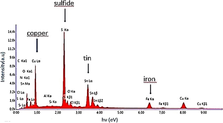
Fig. 1 presents the average elemental composition of CFTS-1, CFTS-2, CFTS-3 and CFTS-4 thin films. We have obtained a surfaces composition rich in sulfur for all films. This behavior may be caused by the crystallization and chalcogenization processes which were performed in sulfur-rich condition in order to minimize its possible loss. CFTS-2 is slightly Cu-rich state, but with further deposition run the films become Cu-poor state. EDX analysis reflects a small variation in tin contents with deposition run. A drastic increase of iron contents with further increase of deposition runs. In the same line, Fig. 1 presents maximum atomic composition of sulfur and tin for CFTS-4. These maximum atomic contents can lead to the formation of some undesirable phases concurrent with CFTS. Fig. 2 shows the EDX image of CFTS-3 with an average composition of Cu:Fe:Sn:S estimated to be 1.87:0.9:1:3.75 which is close to the stoichiometric value of 2:1:1:4 as marked in Fig. 2. It is worthy to mention that physical properties and conversion efficiency of solar cells are deeply affected by atomic composition of materials. As reported elsewhere (Katagiri et al., 2001; Liu et al., 2010), atomic composition and secondary phases of quaternary chalcogenide thin films such as CZTS can affect their electrical resistivity and mobility. So, it is necessary to control the atomic composition during the deposition phase.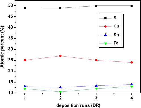
Chemical composition of Cu2FeSnS4 thin films elaborated for different deposition runs (N = 1, 2, 3 and 4).
EDX image of Cu2FeSnS4 thin film prepared for three deposition runs.
3.2 Structural characterization
The XRD pattern of as-sprayed CFTS thin films is illustrated in Fig. 3. XRD diffractograms show all peaks related to stannite CFTS structure (JCPDF card No. 74–1025) with tetragonal space group I
2m. CFTS-1 thin layer is preferentially oriented along (1 1 2) plan was depicted at 2θ = 28.46°. The other peaks were located at 2θ = 31.6°, 47.6° and 56.8° which correspond respectively to (2 0 0), (2 0 4) and (3 1 2) plans. XRD analysis revealed weaker peak of (2 0 0) crystal plane which belongs to the diffraction peaks correspond to quaternary CFTS as cited in (JCPDF card No. 74-1025) Yang et al. (2019). Have been explained this behavior from the repetition of nonplanar units. Also, we can explain the weakness of this (2 0 0) as: The different atomic planes have diverse atomic densities per unit area of the plane, hence, the density of scatterers. At a given atomic plane, the intensities of peaks are proportional to the number of scatterers per unit area. Thus, the peak intensities in the diffractogram will vary. Mostly, when plane indices increased (higher angles in the diffractogram), the intensity of the peak decreases and became narrow. A narrow full-width at half-maximum (FWHM) of preferred orientation of CFTS-3 suggests a significant enhancement of crystallinity. This finding suggests that CFTS-3 might achieved complete growth without post-annealed. Wang et al. (2014) have obtained the same behavior for CFTS nanocrystals synthesized by ultrasound-assisted microwave irradiation. XRD pattern of CFTS-4 shows sharp peak located at 2θ = 26.53° which is related to SnS phase (PDF#75–2112). This undesirable secondary phase is possibly caused by sulfur and tin rich states as shown by EDX results in Fig. 1. This behavior is followed with a slight decrease in preferential peaks intensities. As explained by Seboui and Gassoumi (2014), for CZTS compound, when sulfur amount increases, it becomes to be an electronegative space. Thus, it can react with metal ions leading to create secondary phases.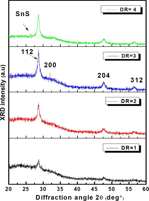
XRD patterns of as- sprayed Cu2FeSnS4 thin films grown at various Deposition runs (N = 1,2,3 and 4).
Table.1 summarized the values of grain size (D), dislocation density (δdis), number of crystallites (Nc) per unit area and strain (ε) of CFTS thin films elaborated at different deposition runs (N = 1, 2 ,3 and 4). D has been increased by an increase of deposition runs to reach a maximum value of about 60 nm at 3 DR. This result proves the enhancement of crystallinity as seen in Fig. 3. This can lead to enhance the conversion efficiency of thin film for solar cells application. Furthermore, δdis was decreased from 25*1010 to 2.77*1010 cm−2 at 3- DR and the Nc was reduced from 3.8*1011 to 0.42*1011 cm−2 at 3 DR. ε was decreased also at 3-DR to minimum value of about 5.66*10−4 which may be due to the enhancement of crystallinity.
Number of DR
D (nm)
δdis × 1011 (cm−2)
Nc × 1011 (cm−2)
ε × 10−4
1
19.60
25.00
3.80
16.00
2
30.30
11.00
2.20
11.00
3
60.00
2.77
0.42
5.60
4
54.20
3.43
0.82
6.20
3.3 Rietveld analysis
Rietveld refinement is a well-known method which provides to calculate structural parameters using diffraction patterns of materials. MAUD software is based on Rietveld analysis to fit the experimental XRD data (Miyauchi et al., 2002). During the fitting process, atomic positions, scale factor, occupancy factors and background coefficients are slightly varied with respecting the experimental XRD spectrum in order to calculate the structural parameters of materials. We can directly extract some information on crystallite size, microstructure parameters and the possible phases that can exist in the sample after fitting process. Fig. 4 shows the Rietveld profile fit of as-sprayed CFTS-3. To obtain good fitting result it is necessary that fitting result (red solid fitting curve) converged rapidly to experimental XRD spectrum (black dots). The high goodness of fitting (GOF) is the relationship between red solid fitting curve and black dots which is equal to 1.08 in our study. There are no additional peaks after fitting process which prove the purity of CFTS-3 phase. Average crystallite size is about 54 nm which is near to the experimental value (D = 60 nm) obtained for (1 1 2) plan (Table 1). Deduced lattice parameters are a = 4.89 Ȧ and c = 8.96 Ȧ which are approximately near to those extracted by JCPDF card No. 74–1025.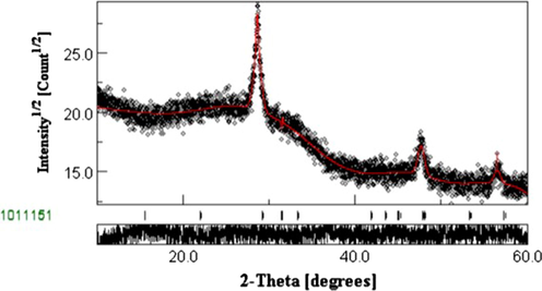
Rietveld refinement of CFTS-3 XRD thin film.
3.4 Raman spectroscopy
It is well known that XRD patterns of chalcogenide Cu2FeSnS4 are close to that of Cu3SnS4 and FeS (Mokurala et al., 2016). Therefore, Raman spectroscopy enables to confirm the phase purity of films and the presence of impurity phases. Fig. 5 presents the Raman spectrum of CFTS-3. We have used 488 nm as excitation wavelength. Raman peaks located at 285 cm−1 and.at 319 cm−1 suggest the phase purity of CFTS-3 as reported by Jiang et al. (2013). The peak depicted at 285 cm−1 is assigned to the sulfur pure anion around Copper cation (Ramanujam Prabhakar et al., 2014). The second peak at 319 cm−1 is assigned to the strongest asymmetry vibration mode of S anion around Sn metal (Ramanujam Prabhakar et al., 2014). We note that CFTS-3 does not present any impurity phase. It is noteworthy to mention that the strong intensity of Raman peak confirms the good crystallinity of CFTS material which is also corroborated with XRD results.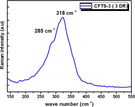
Raman spectrum of Cu2FeSnS4 thin film elaborated by spray pyrolysis at three deposition runs on glass substrates.
3.5 Morphological analysis
In order to explore the surface topography, Scanning Electron Micrographs (SEM) was used to investigate the morphological evolution state of CFTS thin films. Fig. 6 illustrates SEM images of CFTS-1, CFTS-2, CFTS-3 and CFTS-4 thin films grown with the same scale (400 nm). It can be seen that deposition-run process proposed in this work has a notable effect on the films surface morphology. For N = 1, SEM image shows smaller packed particles with the presence of voids. Rectangular shaped is the dominant crystallite structure in this film. This morphology may be related to the sprayed deposition process: at higher temperature, the chemical reaction has a place in the vapor phase resulting by nucleation and the observed crystallite structures. Thus, the grain are formed when fine droplets are deposited on the heated substrate. CFTS-2 thin film has more condensed grains than CFTS-1 with an increase of the size and a change in the form. This behavior may be originated to the coalescence of small grains. CFTS-3 presents a continuous distribution of greater grain particles than CFTS-1 and CFTS-2 with a larger size and a clear defined boundaries are formed. CFTS-3 thin film has compact distribution and large number of micro-aggregates with spherical forms and few voids. This trend may contribute to the enhancement of conversion efficiency in photovoltaic applications as reported elsewhere (Yan et al., 2012; Ben Ali et al., 2016). Also, the increases of volume leads to an increase of film thickness (Ben Ali et al., 2016). At N = 4, the uniformity of CFTS-4 is greatly enhanced. This film shows densely packed grains with compact distribution. Also, the particles aggregated with lower voids than the film grown at three deposition runs.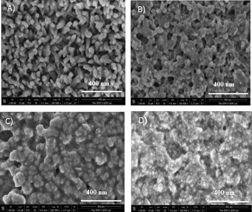
SEM images of Cu2FeSnS4 thin films prepared at A: N = 1, B: N = 2, C:N = 3, and D:N = 4.
3.6 Optical properties
Fig. 7 illustrates the change in transmission T(%), reflection R(%) and absorbance A(%) with the number deposition runs (N). T(%) was decreased with an increase of DR then it increased slightly at 4-DR. CFTS-3 has the lowest transparent quality compared to other films. In the spectral range of 400–2500 nm (Vis-IR), average transmission value decreased appreciably from 30% to a minimum value of 6% at 3-DR. These behaviors are originated by the increase of film thickness. From cross-section method, we have obtained that film thickness of CFTS-1, CFTS-2, CFTS-3 and CFTS-4 are respectively equal to 300, 600, 1.200 and 800 nm. Thicker CFTS-3 film has the lowest transmittance, which may be originated to the presence of bigger crystalline sizes that can decrease the light scattering (Ben Ali et al., 2016). On the other hand, the absorption edges have been shifted to longer-wavelength (red-shift) after increasing deposition runs which suggest that energy band gap has been changed according to the literatures (Yi et al., 2018, 2019). Calculated absorption coefficient value in the visible range of CFTS-3 thin films is about 11·104cm−1. This finding is in good agreement with those published (Guan et al., 2014) and proves the high absorption characteristic of CFTS thin film. Absorbance value A (λ) was shown in Fig. 7. Generally, it could be noted that A(λ) has been increased by an increase of deposition runs. Fig. 7 indicates that the film deposited at 3-DR has the highest A (λ) of about 70% in visible range. This trend can be explained as; when the film thickness increases, grain size increases, as indicated previously; surface morphology grows with compact distribution and few voids which can promote the increase of absorbance values. These obtained results encourage the applicability of CFTS-3 as an absorber material for solar cell application and as catalyst in photocatalysis applications.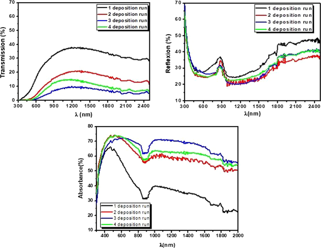
Transmission, Reflexion and Absorbance patterns of CFTS thin films elaborated at various deposition runs.
The plot of (αhν)1/n against (hν) has been determined for different values of n. Optical energy band gap (Eg) values are marked in Fig. 8. Inspection of these figures proves the direct band gap type of CFTS semiconductor. Estimated Eg values were found respectively to be 1.8, 1.67, 1.47 and 1.37 eV for 1, 2, 3 and 4 DR. The energy band gap has been decreased with an increase of DR which is essentially attributed to the increase in energy width of band tails of localized states. This behavior can be seen clearly by the shift of absorption edge as illustrated in transmission spectra (Fig. 7). The variation of Eg with thickness may be due to the changes in crystallinity and purity of the film. Our finding is in good agreement with those published elsewhere (Ramanujam Prabhakar et al., 2014; Jiang et al., 2013).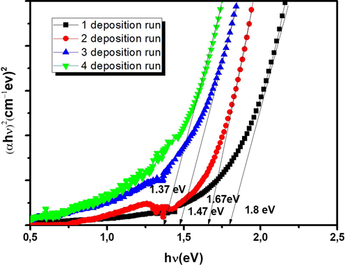
Tauc-plot of the as-sprayed Cu2FeSnS4 thin films elaborated at different deposition runs (N = 1,2,3 and 4).
3.7 Electrical properties
Hall Effect measurements have been performed to determine the electrical properties of CFTS-N thin layers. Table 2 displayed electrical mobility (µ), electrical resistivity (ρ) and volume carrier concentration (Nv) values. CFTS films shows a p-type conductivity. Electrical mobility has been increased to a maximum value of 13.5·102 cm2 V−1 s−1 for CFTS-3. This behavior may be related to the enhancement of crystalline quality (Fig. 3) and surface topography (Fig. 6). Our obtained results are higher than those reported by Mokurala et al. (2016) (7 cm2 V−1 s−1), Ramanujam Prabhakar et al. (2014) (11. 44 cm2 V−1 s−1) and Khadka et al. (0.33 cm2 V−1 s−1) (Khadka and Kim, 2015). An increase of DR leads to enhance the crystalline quality which reinforces contact at the grain boundaries that leads to more free electrons (Rajeshmon et al., 2011; Öztas and Bedir, 2008). At 4-DR electrical mobility has been decreased which can be originate to the presence of SnS as secondary phase and defects. With increasing deposition runs, ρ has been decreased to a minimum value of 5.82 10−3 Ω.cm for CFTS-3 thin layer. As seen from Table 2, Nv has been increased reaching a maximum value of 7.9·1017 cm−3 at 3-DR. This value is higher than that reported by Ramanujam Prabhakar et al. (2014). Electrical results allow to use CFTS-3 thin film as an absorber layer in solar sell devices.
Number of DR
1
2
3
4
µ × 102 (cm2 V−1 s−1)
1.86
1.32
13.50
1.67
ρ (Ω cm)
0.18
4.51 10−1
5.82 1063
1.31
Nv (cm−3)
0.74 1017
1.04 1017
7.90 1017
4.10 1013
3.8 Cyclic voltammetry (CV) analysis
Fig. 9 shows the cyclic voltammetry (CV) curve of CFTS-3 thin film. We have extracted the electrochemical energy levels of CFTS-3 thin layer from the first oxidation onset potentials peak. The valance-band edges (VB) is equal to 0.12 eV. The value of conduction-band energy (CB) was determined from ECB = EVB – Eg which equals to −1.36 eV. Mokurala et al. (2016) have been investigated the electrochemical properties of CFTS and they have been obtained the similar value of VB.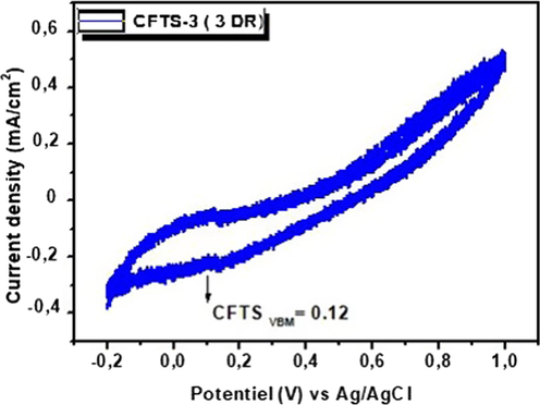
Cyclic voltammogram of CFTS-3 thin film in 0.1 M NaOH and at a scan rate 100 mV/s.
3.9 Photocatalytic activity
Metal sulfide semiconductors with narrow band gaps usually have high ability to absorb the light in visible and near-infrared regions. This permits them to produce as promising photocatalysts of visible light. Promising tendency of combined semiconductors with suitable energy band gaps have been enhanced the photocatalysis efficiency which is originated to the large extent to enhance the separation of photo-induced electrons and holes via interfacial charge transfer (Yang et al., 2009; Gao et al., 2010; Jun Lee et al., 2012; Zyoud et al., 2010). Photocatalytic performances of CFTS-3, SnO2:F ,In2S3, coupled CFTS-3/In2S3, CFTS-3/SnO2:F, and CFTS-3/In2S3/SnO2:F were studied in this part. The process were performed by the degradation of aqueous methylene blue (MB) and aqueous Rhodamine (RhB) solutions as reference pollutants.
3.9.1 Photocatalytic activities of SnO2:F, In2S3 and CFTS-3 thin films
Fig. 10 exhibits the photocatalytic activities of thin films with aqueous MB and RhB solutions under sun light irradiation. The highest absorbance peaks intensity of MB and RhB were matched respectively at 660 nm and 530 nm. The temporal photodegradation of MB dye during 1, 2, 3 and 4 h have a small response for SnO2:F indicates its feeble photocatalysis ability. It could be noted that In2S3 thin layer exhibits higher photocatalytic activity than SnO2:F, but it still lower for removal organic pollutants in waste water. The lower photocatalysis activities of SnO2:F and In2S3 under visible light irradiation are related to their wide energy band gaps and their lower absorbance ability. Under visible light, the electrons can’t jump from the VB to the CB of films. It was reported elsewhere (Habibi and Talebian, 2007) that the degradation rate of dyes was controlled by film thickness. Nevertheless, the photocatalytic efficiency is more important with thicker film which related to the increase in charge carrier concentrations. So, for this reason we have chosen optimum CFTS-3. The degradation of MB dye by CFTS-3 thin film was very important than SnO2:F and In2S3 thin films. From Fig. 10, we can conclude that the degradation of RhB follows the order; SnO2:F < In2S3 < CFTS-3. The photocatalysis reaction mechanism can be described as follows (eqs (a)-(d)) (Enesca et al., 2016):
Photocat + MB (or RhB) → Photacat…MB (or RhB) (Adsorption)(a)
Photocat + hν → e− + h+(b)
h+ (Photocat) + H2O → •OH (Photocat) + H+(c)
MB + •OH → Degradation Products(d)
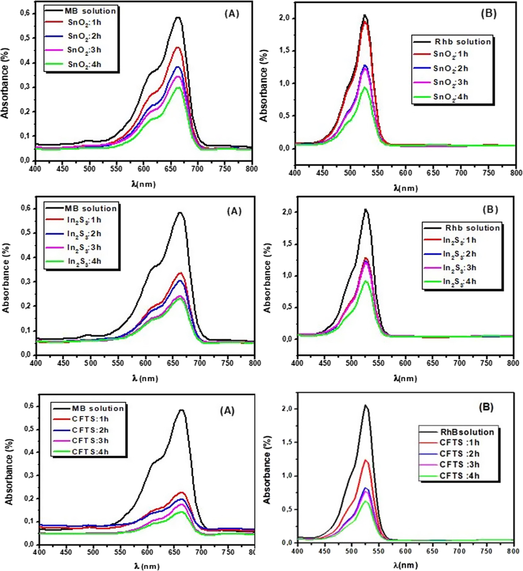
The temporal change of MB (A) and RhB (B) photodegradation for (1, 2, 3 and 4 h) with SnO2:F, In2S3 and CFTS-3 thin films.
3.9.2 Photocatalytic activities of coupling CFTS-3/SnO2:F,CFTS-3/In2S3 and CFTS-3/In2S3/SnO2:F
As proven by many works (Gao et al., 2010; Jun Lee et al., 2012; Zyoud et al., 2010; Zhang et al., 2011) that coupling absorber layer with semiconductor have wide band gap is an advanced technique disciplined to improve; the light-absorbing property in visible region of oxide materials and the photocatalysis performance of absorber layers. Absorber film with narrow band gap has acted as sensitizer (Poongodi et al., 2015). Fig. 11 shows the degradation of MB and RhB solutions by coupling films. This figure indicates that the photoctalysis response of CFTS-3/In2S3 is better than that of CFTS-3/SnO2:F. This behavior may be due to the consequence of electron-transfer process via interface from the CB of In2S3 to that of CFTS. The photocatalytic action mechanism was detailed by measuring the VB and CB potentials of all films. We note also that aqueous MB solution was more decolorized than RhB solution.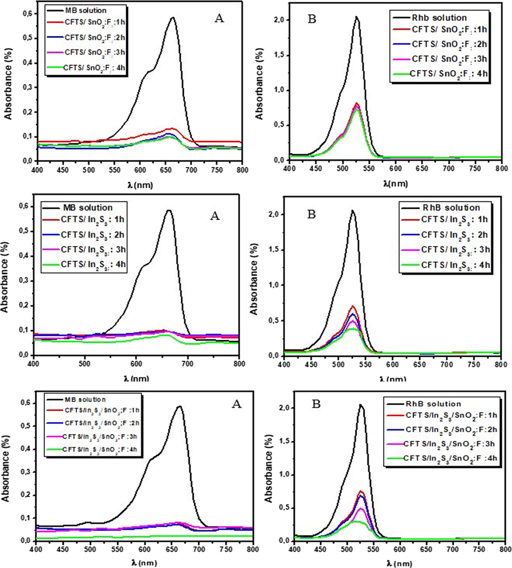
The temporal change of MB (A) and RhB (B) photodegradation for (1, 2, 3 and 4 h) with coupled CFTS-3/SnO2:F, CFTS-3/In2S3 and CFTS-3/In2S3/SnO2.
The calculated valence edges of SnO2:F and In2S3 are located respectively at 3.96 and 3,36 eV. The conduction band edges of SnO2:F and In2S3 are depicted respectively at −0.1 and −0.11 eV. From cyclic voltammetry, valance-band edge of CFTS-3 is 0.12 eV and the value of conduction-band edge is −1.36 eV. As result, we can utilize CFTS-3 as sensitizer and SnO2:F or In2S3 work as a substrates in coupling system. The excellent photocatalysis performance by coupling three films can be described as (Zhang et al., 2011): CFTS-3 has narrow band gap, so the electron in its VB can jumped to its CB with the generation of similar contents of holes on its VB. The photogenerated electrons in CB of CFTS can achieve the CB of In2S3 (or SnO2:F) by reason the more positive conduction band of In2S3 (or SnO2:F) than that of CFTS-3. Consequently, the photogenerated holes can jump from the VB of In2S3 (or SnO2:F) to the VB of CFTS-3. Thusly, the efficient charge separation can improve the lifetime of charge carriers. Also, it can enhance the interfacial charge transfer efficiency via adsorbed substrates. Therefore, photogenerated electron can rapidly jump to the surface of In2S3 (or SnO2:F) and holes on CFTS-3 surface then improving the degradation process of dyes.
Fig. 12 presents a schematic diagram of the band potential of CFTS-3, In2S3 and SnO2:F thin films. The best charge separation was obtained for CFTS-3/In2S3 /SnO2:F heterojunction.. The photogenerated holes from valence band of SnO2:F are promoted to that of In2S3 which works as transitory energy level to valence band of CFTS-3. Under sun light irradiation (Enesca et al., 2016), electrons-hole pairs produced inside the charge space region can be detached by the electric field. Fig. 11 shows the photocatalytic efficiency of CFTS-3/In2S3/SnO2:F heterojunction in aqueous MB and RbB solutions. Calculated photodegradation rate of MB (or RhB) after 4 h in the presence of CFTS-3/In2S3/SnO2:F, CFTS-3/In2S3, CFTS-3/SnO2:F, CFTS-3 , In2S3 and SnO2:F are respectively equals to 96% (or85%), 86% (or81%), 82% (or70%), 76% (or64%), 60% (or53%) and 48% (or53%). MB solution with coupled CFTS-3/In2S3/SnO2:F was decolorized with a value of 96% proves it is higher activity to remove organic pollutants in water. Fig. 13 presents a schematic diagram of photodegradation rate of MB (or RhB) after 4 h in the presence of CFTS-3/In2S3/SnO2:F (green), CFTS-3/In2S3 (pink), CFTS-3/SnO2:F (turquoise), CFTS-3 (blue), In2S3 (red) and SnO2:F (black). From this figure, we evaluate the capacity of different materials to the degradation of MB (or RhB) dye. As seen from this figure, CFTS-3/In2S3/SnO2:F (green), CFTS-3/In2S3 (pink) and CFTS-3/SnO2:F (turquoise) have a great activities to decolorize the dyes than CFTS-3 (blue), In2S3 (red) and SnO2:F (black) thin films.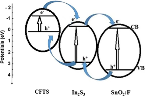
Diagram of the band potential and vectorial charge transfer in the coupling CFTS-3/In2S3/SnO2:F.
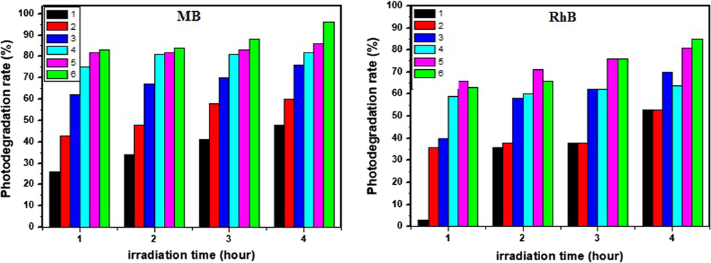
The variation photodegradation rate of MB and RhB with: (1) SnO2:F(black), (2) In2S3 (red), (3) CFTS-3(blue), (4) CFTS-3/SnO2:F (turquoise), (5) CFTS-3/In2S3 (pink), and (6) CFTS-3/In2S3/SnO2:F(green).
4 Conclusion
In summary, chalcogenide Cu2FeSnS4 thin films elaborated based on spray pyrolysis technique at different deposition runs (N = 1, 2, 3 and 4). XRD results showed that crystalline quality and crystallite size have been enhanced. Raman spectroscopy confirms the purity of CFTS-3 phase. Optical band gap energy is equal to 1.47 eV. Hall Effect measurements revealed that a minimum resistivity value of 5.82 10−3 Ω cm is obtained for CFTS-3. Additionally, a high rate value of photocatalytic activity by coupled CFTS-3/In2S3/SnO2:F has been achieved to degrade MB and RhB pollutant solutions under sun illumination. The photodegradation rate was about 96% at 4 h. This result demonstrates that CFTS-3/In2S3/SnO2:F heterojunction structure should be considered a very good candidate to implement eco-friendly, sun-powered devices for removing organic pollution in waste water. We have tested deposition runs method in order to predict the industrialization of the film layers at low cost based on the simple and inexpensive spray pyrolysis technique. So we have supposed that the multi-deposition effect can improve the growth of film without using post-annealed and the films might achieved complete growth without post-annealed.
References
- Gowthami, V., Perumal, P., Sivakumar, R., Sanjeeviraja, C., 2014. Structural and optical studies on nickel oxide thin film prepared by nebulizer spray technique. DOI: http://dx.doi.org/10.1016/j.physb.2014.06.030
- Chatterjee, S., Pal Amlan, J., 2017. A solution approach to p-type Cu2FeSnS4 thin-films and pn-junction solar cells: Role of electron selective materials on their performance. Sol. Energy Mater. Sol. Cells, vol. 160, pp. 233–240.
- Ajili, M., Castagné, M., Kamoun Turki, N.,2015. Spray solution flow rate effect on growth, optoelectronic characteristics and photoluminescence of SnO2:F thin films for photovoltaic application, vol. 126, pp. 708–714.
- Akkari, A.,Reghima, M.,Guasch, C., Kamoun-Turki, N., 2012. Effect of copper doping on physical properties of nanocrystallized SnS zinc blend thin films grown by chemical bath deposition. J. Mater. Sci., vol. 74, pp. 1365–1371.
- Ben Ali, M., Bouaifel, F.B., Sieber, B., Elhouichet, H., Addad, A., Boussekey, L., Férid, M., Boukherroub, R., 2016. Preparation and characterization of Ni-doped ZnO-SnO2 nanocomposites: application in photocatalysis. Superlatt. Microstruct. 10.1016/j.spmi.2016.01.014.
- Structural and optical properties of Cu 3 SbS 3 thin film deposited by chemical bath deposition along with the degradation of methylene blue. Surf. Coat. Technol.. 2018;333:195-200.
- [CrossRef] [Google Scholar]
- Solar-activated tandem thin films based on CuInS2, TiO2and SnO2in optimized wastewater treatment processes. Appl. Catal. B: Environ.. 2016;186:69-76.
- [Google Scholar]
- Solar-activated tandem thin films based on CuInS2, TiO2and SnO2inoptimized wastewater treatment processes. Appl. Catal. B: Environ.. 2016;186:69-76.
- [Google Scholar]
- Williamson, G.B., Smallman, R.C., 1956. Dislocation densities in some annealed and cold-worked metals from measurements on the X-ray debyescherrer spectrum. Philos. Mag., vol. 1, 34.
- Preparation and visible-light photocatalytic activity of In2S3/TiO2 composite. Mater. Chem. Phys.. 2010;122:183-187.
- [Google Scholar]
- Structural and optical properties of Cu2FeSnS4 thin film synthesized via a simple chemical method. Mater. Sci. Semicond. Process.. 2014;25:159-162.
- [CrossRef] [Google Scholar]
- Photocatalytic degradation of an azo dye X6G in water: A comparative study using nanostructured indium tin oxide and titanium oxide thin films. Dyes Pigm.. 2007;73(2):186-194.
- [CrossRef] [Google Scholar]
- Environmental Applications of Semiconductor Photocatalysis. Chem. Rev.. 1995;95(1):69-96.
- [CrossRef] [Google Scholar]
- Houas, Ammar, Lachheba, Hinda, Ksibi, Mohamed, Elaloui, Elimame, Guillard, Chantal, Herrmann, Jean-Marie, 2001. Photocatalytic degradation pathway of methylene blue in water. Appl. Catal. B: Environ., vol. 31, pp. 145–157.
- Huang, Haibao., Leung, Dennis Y.C., Kwong, Philip C.W., Xiong, Jing, Zhang, Lu., 2013. Enhanced photocatalytic degradation of methylene blue under vacuum ultraviolet irradiation. Catal. Today, vol. 201, pp. 189–194.
- Properties of Cu (In, Ga)Se2 solar cells with new record efficiencies up to 21.7%. Phys. Status Solidi RRL. 2014;1–4
- [CrossRef] [Google Scholar]
- Solvothermal synthesis of highly crystallized quaternary chalcogenide Cu2FeSnS4 particles. Mater. Lett.. 2013;102-103:39-42.
- [CrossRef] [Google Scholar]
- Jothibas, M., Manoharan, C., Ramalingam, S., Dhanapandian, S., Bououdina, M., 2014. Spectroscopic analysis, structural, microstructural, optical and electrical properties of Zn-doped In2O3 thin films. Spectrochim. Acta Part A:Mol. Biomol. Spectrosc., vol. 122, pp. 171–178.
- Jun Lee, W., Min Lee, J., Thomas Kochuveedu, S., Hee Han, T., Young Jeong, H., Park, Moonkyu, Moon Yun, J., Kwon, J., Kwangsoo, Ha Kim, D., Ouk Kim, S., Biomineralized N-Doped CNT/TiO2 Core/Shell Nanowires for Visible Light Photocatalysis. ACS Nano, vol. 6, pp. 935–943, DOI: 10.1021/nn204504h.
- J. Appl. Phys.. 2001;40:500-504.
- Structural, optical and electrical properties of Cu2FeSnX4 (X = S, Se) thin films prepared by chemical spray pyrolysis. J. Alloys Comp.. 2015;638:103-108.
- [Google Scholar]
- Liu, F., Li, Y., Zhang, K., Wang, B., Yan, C., Lai n, Y., Zhang, Z., Li, J., Liu, Y., 2010. Sol. Energy Mater. Sol. Cells, vol. 94, pp. 2431–2434.
- Sulfurization temperature dependence of the structural transition in Cu2FeSnS4-based thin films. Mater. Lett.. 2015;161:427-430.
- [CrossRef] [Google Scholar]
- Photocatalysis and Photoinduced Hydrophilicity of Various Metal Oxide Thin Films. Chem. Mater.. 2002;14(6):2812-2816.
- [CrossRef] [Google Scholar]
- Alternative quaternary chalcopyrite sulfides (Cu2FeSnS4 and Cu2CoSnS4) as electrocatalyst materials for counter electrodes in dyesensitized solar cells. J. Power Sources. 2016;305:134-143.
- [Google Scholar]
- Effect of sprayed volume on physical properties of Cu2FeSnS4 thin films and an efficient p-type Cu2FeSnS4/n-type F-doped SnO2 heterojunction. J. Phys. Chem. Solids 2020
- [CrossRef] [Google Scholar]
- Ozel, F., 2016. Earth-abundant quaternary semiconductor Cu2MSnS4 (M ¼ Fe, Co, Ni and Mn) nanofibers: Fabrication, characterization and band gap arrangement. J. Alloys Comp., vol. 657, pp. 157–162.
- Thickness dependence of structural, electrical and optical properties of sprayed ZnO:Cu films. Thin Solid Films. 2008;516(8):1703-1709.
- [CrossRef] [Google Scholar]
- Studies on visible light photocatalytic and antibacterial activities of nanostructured cobalt doped ZnO thin films prepared by sol–gel spin coating method. Spectrochim. Acta Part A Mol. Biomol. Spectrosc.. 2015;148:237-243.
- [CrossRef] [Google Scholar]
- Role of precursor solution in controlling the opto-electronic properties of spray pyrolysed Cu2ZnSnS4 thin films. Sol. Energy. 2011;85:249-255.
- [Google Scholar]
- Ramanujam Prabhakar, R., Huu Loc, N., Hemant Kumar, M., Boix, P.P., Juan, S., John, R.A., Batabyal, S.K., Helena Wong, L., 2014. Facile Water-based Spray Pyrolysis of Earth-Abundant Cu2FeSnS4 Thin Films as an Efficient Counter Electrode in Dye-Sensitized Solar Cells. ACS Appl. Mater. Interfaces, vol. 6, pp. 17661−17667. dx.doi.org/10.1021/am503888v.
- Effect of deposition runs on the physical properties of In2S3 chemically synthesized for photocatalytic application. Results Phys.. 2018;10:706-713.
- [CrossRef] [Google Scholar]
- Seboui, Z., Gassoumi, A., Kamoun-Turki, N., 2014. Evolution of sprayed Cu2ZnSnS4. Mater. Sci. Semicond. Process., vol. 26, pp. 360–366.
- Wang, W., Shen, H.L., Yao, H.Y., Li, J.Z., 2014. Preparation and properties of Cu2FeSnS4 nanocrystals by ultrasound-assisted microwave irradiation. Mater. Lett., vol. 125, pp. 183–186.
- Synthesis and characterizations of quaternary Cu2FeSnS4 nanocrystals. Chem. Commun.. 2012;48(20):2603.
- [CrossRef] [Google Scholar]
- Preparation and photocatalytic activity of high-efficiency visible-light-responsive photocatalyst SnSx/TiO2. J. Solid State Chem.. 2009;182:807-812.
- [Google Scholar]
- Boron nitride quantum dots decorated ultrathin porous g-C3N4: Intensified exciton dissociation and charge transfer for promoting visible-light-driven molecular oxygen activation. Appl. Catal. B. 2019;245:87-99.
- [CrossRef] [Google Scholar]
- Advanced photocatalytic Fenton-like process over biomimetic hemin-Bi2WO6 with enhanced pH. J. Taiwan Inst. Chem. Eng.. 2018;93:184-192.
- [CrossRef] [Google Scholar]
- Synergistic effect of artificial enzyme and 2D nano-structured Bi2WO6 for eco-friendly and efficient biomimetic photocatalysis. Appl. Catal. B. 2019;250:52-62.
- [CrossRef] [Google Scholar]
- Crystal phase-controlled synthesis of Cu2FeSnS4 nanocrystals with a band gap of around 1.5 eV. Chem. Commun.. 2012;48(41):4956.
- [CrossRef] [Google Scholar]
- Cai Zhang, Y., Ni Du, Z., Wei Li, K., Zhang, M., Dionysiou, D.D., 2011. High-performance visible-light-driven SnS2/SnO2 nanocomposite photocatalyst prepared via in situ hydrothermal oxidation of SnS2 nanoparticles. ACS Appl. Mater. Interfaces, vol. 3, pp. 1528–1537,dx.doi.org/10.1021/am200102y.
- Biomolecule-assisted solvothermal synthesis of 3D hierarchical Cu2FeSnS4 microspheres with enhanced photocatalytic activity. Zh. J. Appl. Surf. Sci.. 2015;343:28-32.
- [Google Scholar]
- CdS-sensitized TiO2 in phenazopyridine photo-degradation: Catalyst efficiency, stability and feasibility assessment. J. Hazard. Mater.. 2010;173:318-325.
- [Google Scholar]