

Translate this page into:
Crystal structure, synthesis and characterization of different chromium-based two-dimensional compounds
⁎Corresponding author. m.ruemmeli@ifw-dresden.de (Mark H. Rümmeli)
-
Received: ,
Accepted: ,
This article was originally published by Elsevier and was migrated to Scientific Scholar after the change of Publisher.
Peer review under responsibility of King Saud University.
Abstract
The field of two dimensional (2D) materials experienced a surge of discoveries after the isolation of graphene. Among these, the transition metal compounds of Molybdenum and tungsten have been the most extensively studied materials after graphene. More recently, their group member chromium has only recently come to the limelight after the discovery of its exciting magnetic properties. As such the body of work surrounding 2D chromium-based materials is growing. Here, we present an up-to-date summary of the chromium 2D materials showing the latest advances in their experimental synthesis, characterization and the applications of 2D Chromium-based compounds. Finally, we conclude with a perspective on the future of 2D chromium-based materials. We believe that this study will be helpful to understand the field of chromium-based 2D compounds.
Keywords
Two dimensional chromium
Monolayer chromium
Two dimensional chromium based

1 Introduction
The isolation of graphene generated a new world of two dimensional (2D) materials. The interest in different 2D materials is driven by the virtue of their semiconducting, semi-metallic, insulating, magnetic and numerous other properties that make these materials suitable candidates for numerous different and exciting applications (Khan et al., 2019; Chhowalla et al., 2013). Moreover, these systems can yield Mott insulators, superconductivity, and charge density waves (Gibertini et al., 2019). Today the predicted number of the 2D layered materials has grown to over 5600, of which more than 1800 would be either potentially or easily exfoliated (Ares and Novoselov, 2021). The ever-growing size of the 2D library stresses the need to study the different families constituting the 2D materials in detail with regard to their properties, structure, synthesis methodologies and advanced characterization so as to reap their benefits to the fullest.(See Tables 1 and 2). VdW = Vander Waal, n-VdW = Non vander Waal. Abbreviations in methods: MBE = Molecular Beam Epitaxy, PLD = Pulsed laser deposition, CVT = Chemical Vapor Transport, WS = Wet synthesis, ME = Mechanical Exfoliation, EB = Electron Beam, HPD = High pressure decomposition, AT = Adhesive tape. Abbreviations in Properties: FM = Ferromagnetic, AFM = Antiferromagnetic, SM = Semiconductor.
Formula
Crystal Structure
Space group
CrCl3, CrI3
iMonoclinic
C2/m
CrBr3, Cr2S3
Rhombohedral
R3-
CrO2
Tetragonal
P42/mnm
Crx-Sey
Hexagonal
P63/mmc
CrN
Cubic
Pm3-m
CrP, CrAs, CrSb
Orthorhombic
Pnma
Cr3P
Tetragonal
I4-
Method
Compound
VdW, n-VdW
Substrate
Precursors
Layers No.
Morphology
Properties
Ref
CVD
2D CrS2
Layered
Si
S vapor and Cr
Mono and multilayer
nanoflakes
AFM
(Habib et al., 2019; Wang et al., 2018)
CVD
Cr2S3
n-VdW
Mica
S and CrCl2
Monolayer
nanoflakes
AFM
(Zhou et al., 2019;29(3):1805880.; Cui et al., 2020;32(4):1905896.)
CVD
CrO2
TiO2 (Kang et al., 2015)
CrO3
500 Å-1.2 µm
Thin Films
FM
(Li et al., 1999)
APCVD
CrO2
TiO2(Kang et al., 2015) (Alam et al., 2017) (Constantin et al., 2004) (0 0 1)
CrO3
Thin Films
(Ishibashi et al., 1979)
LPCVD
CrO2
TiO2 (Kang et al., 2015); (0 0 1) (Alam et al., 2017)
CrO3
Thin Films
(Aguilera et al., 2013)
CVD
CrO2
TiO2 (Alam et al., 2017)
CrO3, Cr8O21
Thin Films
(Ivanov et al., 2001; Bullen and Garrett, 2002)
APCVD
CrSe
Non layered
Mica
Se and CrCl3
Monolayer
nanoflakes
FM
(Zhang et al., 2019)
MBE
Cr2Se3
Non layered
Al2O3(0001) Si(Constantin et al., 2004)
Cr and Se
multilayer
Thin Films
AFM
(Roy et al., 2020; Ningrum et al., 2020)
MBE
CrTe2
VdW
GaAs (Constantin et al., 2004)B
Cr and Te
Few layer
Thin Films
FM
(Sun et al., 2021;11(3):035138.)
MBE
Cr3Te4
VdW
pyrolytic graphite
Cr and Te
Monolayer
Thin Films
FM
(Chua et al., 2021)
APCVD
Cr2S3
Non layered n-VdW
Mica
S and CrCl3
Monolayer
Thin Films
FM
(Chu et al., 2019)
CVD
CrS2, CrSe2, CrTe2
sapphire
Cr and Au alloy, chalcogen vapors
Monolayer
Thin Films
FM
(Shivayogimath et al., 2019)
PLD
CrO2
MgO (Kang et al., 2015)
Cr and O2
Multilayer
Thin Films
(Heinig et al., 2007)
CVT
CrPS4
VdW
–
Cr, P, and S powders
–
Thin Films
Capacitors
(Lee et al., (CrPS 4). 2018)
WS
Cr/rGO and MnO
–
Mn(NO3)2·4H2O and Cr(NO3)3·4H2O
–
Powder
Electro-catalyst
(Khan et al., 2019)
AT
Cr2Ge2Te6
260-nm-thick SiO2/Si
Bulk Cr2Ge2Te6
Bilayer
Thin Flakes
(Gong et al., 2017)
ME
CrI3
SiO2/ Si substrate
Bulk CrI3
Monolayer
nanoflakes
SM
(Huang et al., 2017)
ME
CrI3
SiO2/ Si substrate
Bulk CrI3
Bilayer
nanoplatelets
(Zavabeti et al., 2020)
ME
CrSiTe3
SiO2/ Si
bulk
Mono and few layer
nanosheets
FM
(Lin et al., 2016)
EB
NP CrO
Graphene
Cr(C5H7O2)3
Membrane
(Ta et al., 2020)
EB
Cr
Free Standing
Cr(C5H7O2)3
Monolayer
Membrane
AFM
(Ta et al., 2020)
Cr is a transition metal in Group 6 of the periodic table (Fig. 1). It can exist in various oxidation states ranging from −2 to + 6 but the most stable is + 3 (Samadi et al., 2018). In its elemental or uncombined state, chromium is antiferromagnetic at room temperature (Koroleva et al., 2009;153:012057.). Layered as well as non-layered compounds are prominent members of chromium family. Nevertheless, this member of the 2D material family has been long overshadowed by its neighbors i.e., Molybdenum and tungsten which led to the relatively late realization of the unconventional properties of chromium-based 2D materials such as giant tunneling magnetoresistance and a wide range of magnetic behaviors (Song et al., 2018; Gong et al., 2017; Chu et al., 2019; Ta et al., 2020). Still, most of the available scientific literature on chromium-based materials discuss these under the umbrella of contemporary magnetic compounds. A detailed literature, to the best of our knowledge, focusing on chromium-based 2D materials, their crystal structure, properties, and fabrication strategies is missing.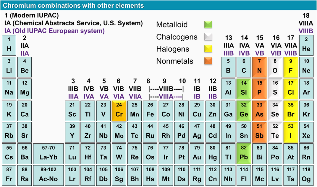
Periodic table highlighting the different 2D combinations of Cr with other elements.
This review article provides a detailed study of chromium-based 2D material and compiles state of the art developments in this 2D family with particular emphasis on the material sub-classes and their crystal structure, and, their synthesis and characterization techniques. At the end we review potential applications of these 2D compounds in fields such as spintronics, biomedicine, and fuel cells are discussed in brief. Finally, future perspectives in the field of the chromium 2D family area also provided. First, we start with the different 2D compounds of chromium that it forms with other elements (Fig. 1),
First, we start with the different 2D compounds that chromium forms with other elements in the periodic table. The compounds are categorized using the name of the family to which the elements belong in the periodic table.
2 Chromium Trihalides, CrX3 (X = F/Cl/Br/I)
Chromium Trihalides (CrX3) are van der Waals layered compounds that are semiconducting in nature. The ferromagnetic semiconducting property of the family was discovered in 1960 while studying CrBr3, though the CrX3 family has still not been well studied. In CrX3 crystals, the Cr atom exists in + 3 oxidation state. Cr ions are arranged in a honeycomb lattice in an edge-sharing octahedral geometry where each ion is further coordinated by six halide (X−) ions (McGuire et al., 2015) Thus, CrX3 layers stack with van der Waals gaps separating these layers. Consequently, the resultant structure is determined by the stacking sequence and relative distance between the layers (McGuire et al., 2015). Notably, in this family CrF3 has hardly been studied in the literature and, it has been experimentally noted that it adopts the R3̅c phase (Knox, 1960). At low temperature all CrX3 (X = Cl, Br, or I) except CrF3, adopt a rhombohedral BiI3 like crystal system (space group R3̅) that upon warming transforms into a monoclinic AlCl3 type system having C2/m space group(Zhang et al., 2015). However, at room temperature the preferred geometry for CrCl3 and CrI3 is monoclinic while CrBr3 has a rhombohedral crystal system. First-principle, calculations predict all CrX3 (X = F, Cl, Br, or I) without exception to have a smaller cleavage energy than graphite; hence, they can be exfoliated as atomically thin 2D materials from their bulk phases (Liu et al., 2016). Moreover, their respective mono layers have high in-plane stiffness, suggesting that they do not curve easily and are stable(Zhang et al., 2015). At ambient temperature and pressure, CrCl3 and CrBr3 have relatively greater air stability than CrI3 (Zhang et al., 2019; Kazim et al., 2020).
CrX3 have strong intraplanar ferromagnetic coupling; but their nature varies (McGuire et al., 2015; Zhang et al., 2015). For example, in CrCl3 the interplanar coupling is antiferromagnetic with a Neel temperature of 16.8 K. Even so, CrCl3 layers can be aligned ferromagnetically in the direction of an externally applied magnetic field of only a few kilooersted (McGuire et al., 2015). On contrary, in CrBr3 and CrI3, the layers stack ferromagnetically with Curie temperatures (Tc) of 37 and 61 K, respectively. Unlike CrCl3, the Cr ions in CrBr3 and CrI3 have moments directed normal to the CrX3 layers and more magnetic anisotropy is observed in their magnetically ordered state (McGuire et al., 2015; Zhang et al., 2015). CrBr3 bilayers retain ferromagnetic behaviors. Contrary to this, CrI3 bilayer is antiferromagnetic (Zhang et al., 2019; Huang et al., 2017). Nevertheless, a large linear magnetoelectric effect is observed in the bilayer CrI3, which makes its magnetism electrically controllable(Jiang and Shan, 2018). Besides, density functional theory studies predicts that CrX3 (X = Cl, Br, and I) can undergo a phase transition from a ferromagnetic to an antiferromagnetic state upon application of compressive strain(Webster and Yan, 2018). The structural information of monolayer CrX3 (X = Cl, Br, and I) is shown in Fig. 2a.![(a) Atomistic structure of monolayer CrX3 (X = Cl, Br, or I). a) Top view of a single layer. Reproduced with permission from Ref. (Webster and Yan, 2018) Copyright 2018, American Physical Society. (b) Single-layer CrS2 with 2H (top) and 1 T (bottom) structures. Cr and S are represented by the blue and yellow balls, respectively. Reprinted from Ref. (Zhuang et al., 2014) [APPLIED PHYSICS LETTERS 104, 022,116 (2014)] with the permission from AIP Publishing (c) Structural model of a CrSe crystal. Reproduced with permission from Ref. (Zhang et al., 2019). Copyright 2019, John Wiley and Sons (d-f) Structural models of rhombohedral Cr2S3. d) Perspective view and e) top view showing the periodic stack of the fully filled “CrS” layer and partially filled “Cr1/3S” layer. The stacking along the z-direction with an A–B–C sequence induces a rhombohedral Cr2S3. Blue, orange, and purple balls represent Cr atoms with different occupancies in the structure. Yellow balls denote S atoms. The entire structure is composed of CrS6 octahedras, in which (f) interlayer octahedras are connected by faces, whereas the intralayer octahedras are connected by edges. Reproduced with permission from Ref. (Zhou et al., 2019;29(3):1805880.). Copyright 2018, John Wiley and Sons.](/content/184/2023/16/8/img/10.1016_j.arabjc.2023.104973-fig2.png)
(a) Atomistic structure of monolayer CrX3 (X = Cl, Br, or I). a) Top view of a single layer. Reproduced with permission from Ref. (Webster and Yan, 2018) Copyright 2018, American Physical Society. (b) Single-layer CrS2 with 2H (top) and 1 T (bottom) structures. Cr and S are represented by the blue and yellow balls, respectively. Reprinted from Ref. (Zhuang et al., 2014) [APPLIED PHYSICS LETTERS 104, 022,116 (2014)] with the permission from AIP Publishing (c) Structural model of a CrSe crystal. Reproduced with permission from Ref. (Zhang et al., 2019). Copyright 2019, John Wiley and Sons (d-f) Structural models of rhombohedral Cr2S3. d) Perspective view and e) top view showing the periodic stack of the fully filled “CrS” layer and partially filled “Cr1/3S” layer. The stacking along the z-direction with an A–B–C sequence induces a rhombohedral Cr2S3. Blue, orange, and purple balls represent Cr atoms with different occupancies in the structure. Yellow balls denote S atoms. The entire structure is composed of CrS6 octahedras, in which (f) interlayer octahedras are connected by faces, whereas the intralayer octahedras are connected by edges. Reproduced with permission from Ref. (Zhou et al., 2019;29(3):1805880.). Copyright 2018, John Wiley and Sons.
3 Chromium chalcogenides
Chromium chalcogenides are a sundry family, that can exist in different stoichiometric compositions. However, the most common ones are CrY2, Cr2Y3, and Cr3Y4. In CrY2 (where Y represent O/S/Se or Te). Starting with chromium dioxide (CrO2), it is a metallic ferromagnetic oxide that crystallizes in the tetragonal rutile structure (P42/mnm space group). Here Cr positions at the center of an octahedral cage that is formed by six oxygen atoms (Cai et al., 2013; Sousa et al., 2007). The electrical resistivities of single-crystal CrO2 and epitaxial thin films are reported to be approximately 250 and 400 µΩ cm, respectively, at room temperature while its curie temperature has been reported as 395 K (Cho, 2003). In different studies conducted, a Dirac electronic phase has been predicted at the interface in thin films and superlattice configurations of CrO2 and TiO2 heterojunctions (Cai et al., 2013; Wang et al., 2015). CrO2 stability is significantly influenced by temperature and oxygen pressure during its preparation. CrO2 is metastable at atmospheric pressure, it decomposes into an insulating antiferromagnetic Cr2O3 when it is heated above 200 °C (Audier et al., 2010). The other competing oxides are CrO3, Cr2O5, and Cr3O4; but Cr2O3 is the most stable among these (a = 4.951 Å; c = 13.566 Å; space group: R3c) (Ivanov et al., 2001; Rabe et al., 2001).
Coming to the next member of chromium dichalcogenides, Chromium disulphide (CrS2) is a material possessing piezoelectric coupling, valley polarization, and dependent intrinsic magnetic properties (Habib et al., 2019; Zhuang et al., 2014). Like other VI transition metal dichalcogenides (TMDs), the Cr layer in CrS2 is also sandwiched between two S layers. Based on the coordination number of Cr, CrS2 can adopt three different phases: Viz 2H (or trigonal prismatic), 1 T (or octahedral geometry), and 1 T′ (or distorted octahedral geometry). In the 2H phase (Fig. 2b top), Cr and S atoms form ABA stacking, where A and B denote the S and Cr atoms, respectively. The 1 T-CrS2 (Fig. 2b bottom) is characterized by the ABC sequence, where one S layer (C) is shifted compared to the others. The 1 T’ phase of CrS2 arises from the dimerization of the 1 T phase. Like MoS2, 2H CrS2 mono-layer is semiconducting, whereas 1 T-CrS2 mono-layer is metallic (Habib et al., 2019; Zhuang et al., 2014). 1 T’-CrS2 is semi-metallic with an approximate bandgap of 10 meV (Habib et al., 2019). Theoretical calculations show that 2H CrS2 is a nonmagnetic semiconductor; whereas 1 T’ CrS2 and 1 T exhibit 2.206 and 0.531 μB magnetic moment per Cr atom, respectively. Moreover, it has been reported that 1 T-CrS2 switches from antiferromagnetic to ferromagnetic property when going from a monolayer to bilayer or thicker CrS2 (Wang et al., 2018). CrS2-based field-effect transistors exhibit p-type behavior (Habib et al., 2019).
Progressing the discussion to chromium tellurides; these exhibit ferromagnetic properties (Dijkstra et al., 1989; Yamaguchi and Hashimoto, 1972; Wang et al., 2018). Monolayer CrTe2 is a 2D ferromagnet; though, it is metastable in bulk, and its multilayers decompose into intercalating compounds i.e., preferably Cr3Te4 or Cr2Te3 (Lasek et al., 2020). The 1 T-CrTe2 phase can be successfully grown only as a monolayer, where the hexagonal Cr planes are sandwiched between Te layers. The CrTe2 layers stack via van der Waals interactions (Lasek et al., 2020; Sun et al., 2021;11(3):035138.; Otero Fumega et al., 2020). The d electrons of Cr provide a non-zero magnetic moment and the emergence of a charge density wave phase in monolayer 1 T-CrTe2, indicating that this phase is the ground state at any strain value in the single-layer limit (Otero Fumega et al., 2020). Moreover; monolayers of Cr3Te4 and Cr2Te3 with room-temperature ferromagnetism and improved Tc, respectively, have also been reported (Chua et al., 2021; Lee et al., 2021). Compared to S and Se, Te has a larger ionic radius that results in the broadening of its d orbitals. Therefore, transition metal tellurides have a smaller bandgap, which makes these compounds a better option for optoelectronic applications in the infrared wavelength range (Su et al., 2019).
Among the chromium chalcogenides of Cr2Y3 stiochiometry, rhombohedral Cr2S3 (Fig. 2d-f) is an extensively studied antiferromagnetic, non-van der Waals material with a Neel temperature of ≈120 K, which is significantly greater than the Tc of CrI3, making it a suitable candidate for future magnetic applications (Zhou et al., 2019;29(3):1805880.). It was established that the conductive properties of Cr2S3 vary with increasing thickness from p-type to ambipolar and then to n-type (Cui et al., 2020;32(4):1905896.). Similarly, Cr–Se is another member of this category occurring in diverse stable stoichiometries such as Cr7Se8, Cr5Se8, Cr3Se4, Cr2Se3, and CrSe. All these compounds have a hexagonal NiAs structure (space group P63/mmc) (Roy et al., 2020), with have varying magnetic properties (Polesya et al., 2013). For instance, CrSe is a non-van der Waals material with clear ferromagnetic properties at temperatures below 280 K (Ningrum et al., 2020; Zhang et al., 2019). On the contrary, Cr2Se3 is an antiferromagnet with a Neel temperature of 43 K (Adachi et al., 2007). The crystal structure of CrSe could be considered as two CrSe2 layers stacked together by a layer of Se atoms; as shown in Fig. 2c.
4 Chromium pnictides
Chromium can form binary compound with pnictides (the nitrogen family). Theoretically, all hexagonal monolayers of chromium pnictides CrZ (Z = P, As, Sb or Bi) have been predicted to be dynamically stable and they possess half-metallic ferromagnetic characteristics with the Tc above the room temperature as well as spin-dependent transport properties (Mogulkoc et al., 2020;102(2):024441.).
Starting with chromium nitride (CrN), it exhibits good corrosion, wear, and oxidation resistance. It has a face-centered cubic lattice at room temperature with paramagnetic properties. Nonetheless, the structure undergoes orthorhombic distortion and becomes an antiferromagnet below the Neel temperature (273 K) (Mogulkoc et al., 2020;102(2):024441.; Era et al., 2005). In CrN films, there is a predominant phase transformation to the hexagonal crystal structure of Cr2N at temperatures above 700 °C. However, at temperatures below 550 °C, the films formed were polycrystalline (Gharavi et al., 2018;51(35):355302.). It is concluded that this transition at lower temperatures is a stress-relaxation-induced phase transformation (Chen, 2003). CrN is semiconducting, having a seebeck coefficient of −230 µVK−1 at 600 K and a high power factor of 5.0 × 10⁻³ Wm−1 K−2 for single-phase CrN at room temperature (Gharavi et al., 2018;51(35):355302.). In contrast to CrN, Cr2N is metallic, with a seebeck coefficient of few µVK−1 and thermal conductivity of 12 W m−1 K−1 at room temperature, which is approximately 4.0 W m−1 K−1 for CrN (Gharavi et al., 2019). The phase shift between CrN and Cr2N can be controlled by the deposition temperature and partial pressure of the nitrogen gas flow (Hones et al., 1997).
Chromium phosphide (CrP) is yet another member of this family that having orthorhombic lattice. It is thermally stable, metallic, and has anti-corrosive and oxidation-resistant properties (Liu et al., 2019; Motojima and Higashi, 1985). Chemically resistant and conductive CrP films have been produced using chemical vapor deposition (CVD) (Blackman et al., 2004). Similarly, another stoichiometry, Cr3P (tetragonal), has also been produced using CVD. These phosphides have potential applications as protective coatings for metals prone to oxidation and in catalysis (Motojima and Higashi, 1985; Blackman et al., 2004).
Coming to the next member of this family, chromium arsenide (CrAs): it has been found to possess superconductive behavior under external pressure. It has an orthorhombic MnP-type crystal structure at ambient temperature (Nigro et al., 2020). Soon after the discovery of CrAs, bulk superconductivity at room temperature was discovered in K2Cr3As3 (Bao et al., 2015). Similarly, three additional superconductors in A2Cr3As3 stoichiometry, where A can be Na, Rb, or Cs, have also been synthesized (Mu et al., 2018; Tang et al., 2015). This family of unconventional superconductors have a quasi-one-dimensional crystal structure with infinite [(Cr3As3)2−]∞ linear chains of double-walled sub-nanotubes interconnected by A + ions (Noce, 2020). The family is still under further investigation for correlation between electronic properties and the reduced dimensionality.
Progressing further in the family; the theoretical investigations on the magnetic properties and electronic structures of CrSb are very rare. Although, the electronic structure of CrSb has been compared with those of CrP and CrAs having a MnP-type structure (Polesya et al., 2013; Ito et al., 2007). Similarly, two dimensional chromium bismuthate (CrBi), is also only theoretically studied member of the family that has been predicted to have a room temperature Ising ferromagnetism with tunable magneto-optical response (Mogulkoc et al., 2021).
5 Chromium-based ternary compounds
Among the ternary compounds of chromium, layered tellurides with the stoichiometric formula CrXTe3 (X = Si, Ge, Sn, Pb) have been extensively studied. These materials have attracted significant research interest as potential candidates for two-dimensional magnets due to their range of magnetic characteristics. For instance, monolayer CrSiTe3 is a robust 2D ferromagnetic semiconductor that forms the basis for spintronics, and it is a good example of a layered telluride with pairs of silicon atoms. It is formed from stacks of Te–(Cr, Si)–Te sandwich layers. Each layer has a Si2Te6 (ethane-like group) with two Cr ions inserted between two layers of Te planes, leading to a van der Waals gap of approximately 3.3 Å. The Cr ions form a honeycomb sublattice with Si pairs at the center of the hexagons (Casto et al., 2015; Lin et al., 2016; Ouvrard et al., 1988). The crystal structure of CrSiTe3 is shown in Fig. 3a (Lin et al., 2016). Using the Heisenberg model, it has been predicted that the Tc of the single-layer CrSiTe3 would significantly shift to higher temperatures compared to its bulk form, and it would increase further when the CrSiTe3 layers are strained (Casto et al., 2015; Lin et al., 2016; Ouvrard et al., 1988; Li and Yang, 2014; Chen et al., 2015). Some Other theoretical calculations predict that the monolayer CrSiTe3 should be antiferromagnetic when the significance of second-and third-order exchange interactions are considered (Sivadas et al., 2015). However, experimental confirmation still lacks.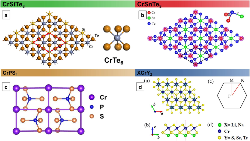
(a) Top views of the atomic structure of a 2D CrSiTe3 monolayer. A unit cell is indicated by the red dashed line. The local atomic structure around Cr, a distorted CrTe6 octa-hedron, is shown on the right. Reproduced with permission from Ref. (Chen et al., 2015). Copyright 2015, Elsevier. (b) Top view of a single-layer CrSnTe3 structure. The solid black line denotes a unit cell of the single-layer CrSnTe3. The spin charge density is also shown with an isosurface of 0.025 e/°A3. Reprinted figure with permission from Ref. (Zhuang et al., 2015) Houlong L. Zhuang, Yu Xie, P. R. C. Kent, and P. Ganesh, PHYSICAL REVIEW B Computational discovery of ferromagnetic semiconducting single-layer CrSnTe3 92, 035,407 (2015) Copyright 2015, American Physical Society (c) Schematic illustration of the atomic structure of CrPS4. Reproduced with permission from Ref. (Lee et al., (CrPS 4). 2018). Creative Commons CC BY license (d) a) Top and b) side views of the relaxed structures of XCrY2 (X = Li and Na; Y = S, Se, and Te) FMS monolayers. c) Brillouin zone of the XCrY2 monolayers. d) The green, purple, and yellow spheres represent alkali metals, Cr, and Y atoms, respectively. Reproduced with permission from Ref. (Xu et al., 2020). Open Access, American Chemical Society.
Similarly, CrGeTe3 is a layered ferromagnetic telluride is structurally similar to CrSiTe3; except for that its Tc (∼61 K) is relatively higher than that of CrSiTe3 (32 K) (Li and Yang, 2014; Tian et al., 2016). Besides, the spins point lies along the c-axis in both materials (Casto et al., 2015; Zhang et al., 2016). The layers in CrGeTe3 were bound together more tightly as compared to those in CrSiTe3. Thus, CrGeTe3 has a smaller band gap of 3.27 °A compared to CrSiTe3 (3.32 °A), resulting in a shrinking effect of the lattice parameter c from CrSiTe3 to CrGeTe3 (Li and Yang, 2014); which could lead to a transition of the magnetic mechanism from 2D to 3D. Additionally, CrGeTe3 has been reported as a substrate for inducing an anomalous quantum Hall effect in the topological insulator Bi2Te3 (Alegria et al., 2014).
The single layer of CrSnTe3 has been predicted to be mechanically and dynamically stable (Fig. 3b) (Zhuang et al., 2015). The formation energy of CrSnTe3 is higher compared to those of CrSiTe3 and CrGeTe3, revealing that it exhibits the strongest interlayer coupling, indicating that the magnetism of CrSnTe3 should be closer to that of the 3D-Ising model (Lin et al., 2017). Yet to date, single-crystalline CrSnTe3 has not been experimentally isolated. Similarly, CrPbTe3 has only been predicted to exist. Its cohesive energy is negative and similar to 2D silicone that suggest that the material should be thermodynamically stable once synthesized (Khan and Hong, 2020).
Chromium thiophosphate (CrPS4) is another 2D-layered ternary compound of chromium (Fig. 3c). It is semiconducting with an energy gap of 0.166 eV and an antiferromagnetic transition temperature of 36 K. CrPS4 crystallizes into a monoclinic crystal system where its lattice has puckered hexagonally close-packed sulfur layers parallel to the bc plane. The Cr and P atoms are coordinated in distorted octahedral and tetrahedral interstices, respectively, by S atoms. A large Vander Waal gap exists between the S layers along the c-axis in the bulk (Pei et al., 2016). The in-plane anisotropy and peculiar metamagnetic transitions make few-layered CrPS4 flakes a promising candidate for studying 2D magnetism and exploring synaptic devices as well as their applications in neuromorphic computing (Lee et al., 2018; Peng et al., 2020; Cao et al., 2021).
Similarly, CrMAs (M = Ni or Rh) is another family of 2D chromium-based ternary compounds with Fe2P-type crystal structures, where Cr atoms occupy pyramidal sites, whereas Ni and Rh are present at tetrahedral sites. The nature of the atoms present at tetrahedral sites is crucial in deciding the magnetic property of the compounds. For instance, CrNiAs is known as a ferromagnet with a Tc of 193 K (Nylund et al., 1972). In contrast, CrRhAs is an antiferromagnet with a Neel temperature of 165 K (Ohta and Kanomata, 1990; Ohta et al., 1995).
Monolayer alkali-based chromium chalcogenides, XCrY2 (X = Na and Li Y = Se, S, and Te), is a theoretically proposed class of ferromagnetic semiconductors (Fig. 3d) (Xu et al., 2020). First-principles calculations predicted the separation of XCrY2 from their bulk crystals to be possible via exfoliation. Using the Ising and Heisenberg models, LiCrSe2, NaCrTe2, and NaCrSe2 were established to exhibit direct band gaps and ferromagnetic ground states with high magnetic curie temperature (Tc). Moreover, the spin–orbit coupling (SOC) effects might significantly change the effective mass of the holes, leading to a higher hole mobility. Furthermore, the high potential difference (ΔV greater than 1.23 eV) between the lower and upper surfaces of the XCrY2 monolayer is suitable for photocatalytic water splitting applications (Xu et al., 2020; Kumari et al., 2021).
6 Mono layer chromium
Owing to their high aspect ratio, large specific area, and unsaturated surface coordination, the freestanding 2D elemental nanosheets of atomic thickness have always been of distinct advantages over their bulk counterparts (Ling et al., 2015). Contrary to van der Waals layered 2D materials, metallic bonding systems support close packed structures, due to which monolayer free standing metallic sheets are challenging, though recent theoretical and experimental studies indicate their existence.
Chromium is archetypal antiferromagnet material, with an incommensurate spin-density wave (SDW). Moreover, it is the only solid having antiferromagnetic ordering below (and at) room temperature that can form paramagnetic ordering above 38 °C. The 3d character of this metal is of fundamental importance, considered the absence of antiferromagnetism in Mo and W. Apart from the rare earths and actinides, in which the localized f electrons are responsible for the magnetic nature, the three elemental antiferromagnets are indeed all 3d metals: i.e., Cr, α-Mn, and γ-Fe (Fawcett, 1988). Antiferromagnetic materials can generate large magneto transport effects, display ultrafast dynamics, they are robust against perturbation due to magnetic fields and produce no stray fields. Thus, Antiferromagnetic materials could represent the future of spintronic applications (Baltz et al., 2018).
Recently, free-standing single-atom-thick crystalline 2D chromium membranes suspended in graphene pores were formed in situ via electron beam irradiation (Fig. 4) (Ta et al., 2020); that reduced CrO to Cr in situ using low-voltage (80 kV) spherical aberration-corrected transmission microscopy (LVACTEM). These Cr membranes exhibiting antiferromagnetic ground states are highly attractive for future spintronic applications and further consolidate the existence of a new class of elemental 2D metals. The lattice constant for the Cr membrane is less than that of the bulk Cr of 2.88–2.91 Å. To the best of our knowledge, so far, this is the first and only report regarding isolation of monolayer Cr.![Schematics for synthesis of Cr membrane via electron beam irradiation. (a) TEM micrograph showing amorphous Cr, O, and C composite film on graphene prior to irradiation. (b) Partial chromium oxide NP with a 2D Cr single-atom-thick membrane. (c) Crystalline single-atom thick Cr membrane with square lattice in a graphene pore. (d) Chromium oxide NP over graphene. Scale bars are 10 nm in (a) and 2 nm in (b − d). Reprinted with permission from Ref. (Ta et al., 2020) Nano Lett. 2020, 20, 6, 4354–4361. Copyright [2020] American Chemical Society.](/content/184/2023/16/8/img/10.1016_j.arabjc.2023.104973-fig4.png)
Schematics for synthesis of Cr membrane via electron beam irradiation. (a) TEM micrograph showing amorphous Cr, O, and C composite film on graphene prior to irradiation. (b) Partial chromium oxide NP with a 2D Cr single-atom-thick membrane. (c) Crystalline single-atom thick Cr membrane with square lattice in a graphene pore. (d) Chromium oxide NP over graphene. Scale bars are 10 nm in (a) and 2 nm in (b − d). Reprinted with permission from Ref. (Ta et al., 2020) Nano Lett. 2020, 20, 6, 4354–4361. Copyright [2020] American Chemical Society.
7 Preparation methodologies
The properties and applications of 2D materials strongly depend up on their crystal structures and morphologies. Therefore, the synthesis and design of 2D materials are crucial to study their potential applications further. Various synthesis strategies such as top-down exfoliation, chemical vapor deposition (CVD), and thermal decomposition have been developed for their synthesis (Dong et al., 2018; Zhou et al., 2018; Xiao et al., 2018). The size, shape, and uniformity of 2D materials can be tuned to a certain extent by reforming experimental conditions such as concentrations, chemical reagents, and temperature.
Transition metal chalcogenides of Mo and W had been the subject of intensive research. Because Cr belongs to the same group of these elements, there is a dire need to study Cr-based materials to put their fascinating properties into potential applications. However, as the 3d orbital of Cr atom contains no radial node and thus its electrons are closer to the nucleus, it makes Cr different as well as a bit difficult from its group members. For Cr based compounds, the lower oxidation states of + 3 and + 2 are stable. On the contrary, owing to the presence of radial nodes in 4d and higher d orbitals, the higher oxidation states of Mo and W are more stable. Thus, the stability of Mo- and W-based compounds is different from those of Cr-based compounds. Consequently, the synthesis strategies that generally work for Mo and W, may not necessarily perform equally well for the synthesis of Cr compounds. Thus, the synthesis methods for fabricating Cr-based 2D materials require special attention and tailoring. The different methods for synthesizing Cr-based 2D compounds are summarized below.
7.1 Chemical vapor deposition (CVD)
CVD has distinct advantages such as high yield, large surface area, and large crystal domains of the product over other synthetic strategies (Dong et al., 2018). CVD is a commonly employed bottom-up synthesis approach for fabricating 2D layered materials, most of which are van der Waal materials. Non-van der Waal materials are non-layered and preferably form 3D bonding, which makes their ultra-thin 2D fabrication difficult through conventional CVD growth. This limitation has been overcome using chemically inert and smooth substrates. Epitaxial growth has shown great success in growing 2D non-layered, non-van der Waal materials using the facile CVD synthesis. Unlike conventional epitaxies, such as molecular beam epitaxy and metal organic CVD, van der Waal epitaxy does not require a lattice match between the growing layer and the substrates. The lattice mismatch can act as a buffer against thermal stress in addition to facilitating the migration of the reaction precursors, resulting in high anisotropic growth with relatively high crystal quality, large lateral sizes, and defect-free crystals (Dong et al., 2018; Zhou et al., 2018). Mica, MoS2, graphene, and h-BN are the examples of commonly used substrates for van der Waal epitaxy substrates because they are atomically smooth and have chemically inert surfaces (Dong et al., 2018).
In general, the CVD growth of Cr-based 2D materials (Fig. 5a) involves the use of a metal precursor either in the form of Cr powder or its halides/oxides that are further reacted with S, Se, or Te for chalocogenization (Habib et al., 2019; Zhou et al., 2019;29(3):1805880.; Li et al., 1999; Ishibashi et al., 1979; Aguilera et al., 2013; Bullen and Garrett, 2002). The crucial parameter in the CVD growth of 2D non-van der Waal materials is to effectively control the concentration of the precursor to prevent the formation of their thermodynamically more stable 3D analogues (Zhou et al., 2019;29(3):1805880.). Therefore, space-confined strategy that accelerates the horizontal rather than vertical growth of samples is generally adopted in addition to the use of van der Waal epitaxy substrates (Utama et al., 2013; Huang et al., 2017). Moreover, the Cr-based 2D non Vander Waal materials can be grown using salt-assisted CVD synthesis (Chu et al., 2019; Zhang et al., 2019). This involves mixing of a metal precursor and salt forms a molten solution that generates intermediate products, thereby increasing the vapor pressure by decreasing the melting point of the reactant (Chu et al., 2019; Han et al., 2019). In addition, the salt can act as a gaseous catalyst that increases the growth rate by decreasing the energy barrier (Zhang et al., 2019). Currently, CVD is the most successful technique for depositing CrO2 thin films that has been used by various authors (Cho, 2003; Sousa et al., 2006; Li et al., 1999; Ishibashi et al., 1979; Aguilera et al., 2013; Bullen and Garrett, 2002),with minor modifications since it was first reported by Isibashi et al (Zhang et al., 2015; Ivanov et al., 2001; Ishibashi et al., 1979; Ishibashi et al., 1978).(See Fig. 6).![Different methods for fabricating the 2D Cr-based materials. (a) Schematic for CVD synthesis of ultrathin Cr2S3 flakes on two stacked mica sheets with CrCl2 and S as the co-evaporation sources. Reproduced with permission from Ref. (Zhou et al., 2019;29(3):1805880.). Copyright 2018, John Wiley and Sons. (b) A general approach for synthesizing thin layers of 2D binary compounds. Reproduced with permission from Ref. (Shivayogimath et al., 2019) Creative Commons CC BY, Springer Nature (c) Schematics of high-Tc Cr2Te3 thin films grown on Al2O3 via molecular beam epitaxy. Reprinted (adapted) with permission from Ref. (Li et al., 2019) [ACS Appl. Nano Mater. 2019, 2, 11, 6809–6817], copyright [2019] American Chemical Society. (d) Scheme for the one-step synthesis and vapor transport of CrX3 (X = Br, I) micro- and nanosheets. Reproduced with permission from Ref. (Grönke et al., 2019). Creative Common License, John Wiley and Sons.](/content/184/2023/16/8/img/10.1016_j.arabjc.2023.104973-fig5.png)
Different methods for fabricating the 2D Cr-based materials. (a) Schematic for CVD synthesis of ultrathin Cr2S3 flakes on two stacked mica sheets with CrCl2 and S as the co-evaporation sources. Reproduced with permission from Ref. (Zhou et al., 2019;29(3):1805880.). Copyright 2018, John Wiley and Sons. (b) A general approach for synthesizing thin layers of 2D binary compounds. Reproduced with permission from Ref. (Shivayogimath et al., 2019) Creative Commons CC BY, Springer Nature (c) Schematics of high-Tc Cr2Te3 thin films grown on Al2O3 via molecular beam epitaxy. Reprinted (adapted) with permission from Ref. (Li et al., 2019) [ACS Appl. Nano Mater. 2019, 2, 11, 6809–6817], copyright [2019] American Chemical Society. (d) Scheme for the one-step synthesis and vapor transport of CrX3 (X = Br, I) micro- and nanosheets. Reproduced with permission from Ref. (Grönke et al., 2019). Creative Common License, John Wiley and Sons.
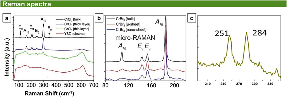
(a) Micro-Raman measurement of bulk CrCl3 (black), CrCl3 nanosheets (thick layer, blue), CrCl3 nanosheets (thin layer, green), and of the pure YSZ substrate (red). (b) Micro-Raman measurement of bulk CrBr3 (black), CrBr3 microsheet (red), and a CrBr3 nanosheet (blue). Reproduced with permission from Ref. (Grönke et al., 2019). Creative Common License, Jhon Wiley and Sons (c) Typical Raman spectrum of CrSe on SiO2/Si. Reproduced with permission from Ref. (Zhang et al., 2019). Copyright 2019, John Wiley and Sons.
In addition to these strategies, another commonly used method involves the use of a gas-phase precursor metallographic limited dissolution technique that enables the synthesis of several Cr-based materials including telluride, selenide, and sulfide by CVD (Shivayogimath et al., 2019). Using this method, few-atom-thick binary compounds can be fabricated by varying the choice of X (=S, Se, Te) and metal, and different compounds can be obtained on the same growth substrate. (Fig. 5b).
7.2 Metal-organic CVD
Metal-organic CVD is the most promising techniques for thin film deposition as evinced by wafer-scale films (Eichfeld et al., 2015; Kang et al., 2015). For the growth of crystalline monolayer TMDs, powder precursors have been commonly used owing to their high reactivity at elevated temperatures and low costs. However, in CVD system, there is lack of control over the powder precursor supply. This limitation can be overcome using metal–organic CVD as it offers controlled precursor flowrates and therefore the growth time can be extended to hours (Och et al., 2021). In general, the metal–organic CVD precursors are required to have high reactivity, high volatility, stability and preferably low toxicity with a key requirement of less carbon content since its leads to accumulation of carbonaceous species on the substrate/product interface besides the product surface.
Among the different precursors used for the synthesis of CrX2 using metal–organic CVD, chromium carbonyl precursor (Cr(CO)6) has a higher volatility rate. Moreover, pyrolysis of chromium carbonyl increase below 500 °C that facilitates films growth on temperature-sensitive substrates as compared to other commercially available complex organo-chromium precursors (Wei and Lo, 1998). For instance, with use of chromium carbonyl, the highest growth rate of Cr2O3 with negligible carbon contamination can be achieved at 500 °C precursors(Carta et al., 2005). Therefore, the use of chromium carbonyl precursors is generally preferred for MOCVD growth of CrX2. Additionally, alkali metals salts are becoming popular precursors owing to increased domain size. Nevertheless, these too cause higher contamination of Na and epitaxy loss in the synthesized films (Kang et al., 2015). In MOCVD, the precursor purity significantly affect the quality of the film produced and difference of 99% and 99.99% becomes significant (Eichfeld et al., 2015). And thus makes MOCVD more expensive.
7.3 Physical vapor deposition (PVD)
Physical vapor deposition (PVD) techniques such as pulsed laser deposition (PLD) and molecular beam epitaxy (MBE) are commonly used for in situ fabrication of multilayer films and for developing high-quality interfaces (Heinig et al., 2007). Various Cr-based materials can be synthesized using these techniques. For instance, thin films of chromium sesquioxide (Cr2O3) on Si have been prepared through pulsed laser deposition (PLD) (Tabbal et al., 2006). In addition, several groups have fabricated CrO2 films on TiO2 (Kang et al., 2015), Si (Constantin et al., 2004), Si (Kang et al., 2015), Al2O3 (0001), and LaAlO3 (Kang et al., 2015) via MBE (Ingle et al., 2001) and PLD synthesis (Shima et al., 2002; Stanoi et al., 2005). Apart from chromium oxides, single-phased chromium oxynitride [Cr(Nx,Oy)] films on Si (Kang et al., 2015) substrates have also been synthesized using the PLD technique. The films structurally resembled CrN; however, the N atoms were partially substituted by oxygen. When different pressures of nitrogen were used in the presence of residual oxygen, it was established that a relatively smooth film surface was obtained when low pressure of nitrogen was used (Suzuki et al., 2002).
Similarly, thin films of CrN have been grown on MgO (0 0 1) substrates using radio-frequency N plasma-assisted MBE (Alam et al., 2017; Constantin et al., 2004). In addition, thin films of Cr2Te3 and Cr2Se3 had been deposited on Si and Al2O3 substrates using MBE (Fig. 5c) (Roy et al., 2020; Roy et al., 2015; Li et al., 2019; Pramanik et al., 2017). Additionally, single layer CrI3 and ternary system of Cr2Ge2Te6 has been prepared using MBE (Li et al., 2020; Mogi et al., 2018).
7.4 Chemical vapor transport (CVT)
CVT is a method for conducting heterogeneous reactions between a reactive gas phase and a condensed phase and it makes use of elevated temperature and temperature gradients (Lenz and Gruehn, 1997; Binnewies et al., 2013). The advantage of CVT is that it requires no additional carrier gas. The use of CVT for the preparation of the Cr-based 2D materials has only recently emerged with reports regarding CrPS4 and CrX3 (X = Cl, Br, or I) synthesis (Lee et al.2018,; Grönke et al., 2019; De Siena et al., 2020), CrX3 (X = Cl, Br, or I) micro- and nanocrystals have been directly deposited on a yttria-stabilized zirconia (ZrO2:Y2O3) substrate in an endothermic process in two-zone furnaces conducted in quartz ampoules (Fig. 5d) (Grönke et al., 2019). Similarly; single-crystal CrPS4 has been grown using Cr, P, and S precursor powders (Lee et al., 2018).
7.5 Atomic layer deposition
Atomic layer deposition (ALD) is a technique that uses gaseous precursors to grow desired films through chemical surface reactions(Leskelä et al., 2014). So far, ALD studies have focused on transition metal dichalcogenides and is a very active and rapidly growing field of research(Mattinen, 2020). For chromium based two-dimensional compounds the use of ALD is not very common. To the best of our knowledge, only CrOx films are commonly deposited using ALD method(Tarre et al., 2008; Jõgiaas et al., 2022; Daresibi et al., 2022). The atomic layer deposition method was used to synthesize CrOx/SiO2 catalysts for oxidation of propane to propylene using CO2. The ALD synthesis method resulted in the higher dispersion of chromium oxide particles and higher specific reaction rates(Daresibi et al., 2022) when compare to CVD method of synthesis.
7.6 Mechanical exfoliation
Mechanical cleavage or the Scotch-tape method is the earliest, easiest, cheapest, and the most commonly used technique for producing mono-or few-layered 2D materials from their bulk counterparts (Samadi et al., 2018). This technique provides high-quality crystalline products with almost no or negligible defects. Besides, the degree of contamination in the product is relatively low as the process does not use chemicals (Zavabeti et al., 2020). Therefore, most of the basic physics and devices on 2D materials rely largely on this method (Choi et al., 2017).
Theoretically, the method can isolate single-layer 2D materials from any crystal with an atomic layered structure yet the method has some practical limitations. For instance, crystals that have ionic bond characteristics or more polar covalent bonds have strong interlayer coupling; therefore, peeling off their single layer from the corresponding natural crystal is difficult. In addition, the shape, size, and thickness of the nanosheets fabricated using this method exhibit random domain sizes and thicknesses and lack repeatability (Zavabeti et al., 2020). Moreover, the repeated transfer process is not scalable for practical purposes (Duan et al., 2015).
8 Structural characterization
After describing the different methods for the 2D chromium-based materials growth, the next step is to identify pathways for the reliable characterization technique required to determine the number of layers of these 2D materials. We review some of the primary techniques used to characterize the structure of Cr-based 2D materials.
8.1 Raman spectroscopy
Raman spectroscopy is a non-destructive characterization tool used to obtain information about the lattice vibrations of 2D crystals. For 2D materials, Raman spectroscopy is a basic tool for extracting information about its layer number. Starting with chromium halides CrX2 (X = Cl, Br, I); micro-Raman study of bulk CrCl3 shows four Eg (at 116.2, 208.6, 247.0, and 345.6 cm−1) and two A1g (at 166.2 and 298 cm−1) vibration modes (Kazim et al., 2020). As the layer number decreases (nanoscale), the peak intensity of the Raman vibrations decreases, and the two peaks lying at the extreme left and right (at 116.2 and 345.6 cm−1) are the first to disappear from the Raman spectrum. In thinner or bilayers, the underlying substrate significantly influences the obtained results, and the only identifiable dominant peak is at 298 cm−1. While for CrBr3, there are four Raman active modes (two Eg at 152.5 and 142 cm−1 and two A1g at 183.5 and 107 cm−1 respectively) (Borghesi et al., 1984). For the micro- and nanosheets of CrBr3, the intensity of the A1g peak at approximately 108 cm−1 significantly decreased as compared to those of the bulk samples. CrI3 nanosheets have extremely strong oxygen sensitivity under ambient conditions, which hinders a comprehensive study of these via micro-Raman (Grönke et al., 2019). Whereas for bulk CrI3, the Raman spectrum constitutes only one lattice vibration of the Ag type at 110 cm−1. For the nano- and micro-layered CrI3, the total intensity of the acquired Raman peaks of were fairly decreased and broadened (Grönke et al., 2019). In some studies, the unpolarized Raman spectrum of bulk CrI3 crystals has been reported to display a series of peaks at frequencies of 77.1, 100–110, 128.4, 231.7, and a weak, broad excitation at 253.2 cm−1 (Shcherbakov et al., 2018).
For Cr chalcogenides, the Raman spectra of the polycrystalline CrO2 films grown on Ti substrates are characterized by the presence of three prominent bands centered at 455 ± 51, 565 ± 5, and 683 ± 5 cm−1 attributed to the vibrational modes Eg, A1g, and B2g of the rutile substrate. Moreover, the orientation of the rutile single crystal with respect to the incident light determines the number of detected bands when examined via Raman spectroscopy. When light imping normally on the rutile (0 0 1) face, all three peaks are allowed. However, the B2g mode would be forbidden when the rutile (Alam et al., 2017) and (Kang et al., 2015) faces were examined (Aguilera et al., 2013). In addition, the type of substrate used to grow CrO2 affects the number of Raman allowed modes. For instance, for CrO2 grown on Al2O3 (0001), B1g (149 cm−1) was active (Stanoi et al., 2005). Pristine Cr2O3 ultra-thin films exhibit a signature peak at 551 cm−1 attributed to the A1g vibration mode (red shifted from its bulk value of 554 cm−1). In addition, Eg modes were observed at 300, 350, 520, and 620 cm−1 (Dutta et al., 2017).
The different stoichiometries of chromium sulfides have similar yet distinguishable Raman features. For all chromium sulfides, the Raman spectra constitute four primary peaks at ca. 175, ca. 253, ca. 285, and ca. 364.0 cm−1 (with ± 10) (Habib et al., 2019; Zhou et al., 2019;29(3):1805880.; Cui et al., 2020;32(4):1905896.). The peak at 253 cm−1 corresponds to the in-plane Eg mode, whereas the other three peaks correspond with the out-of-plane Ag modes. In spite of that, the difference in the strength of the covalent bond between Cr and S atoms affects the Raman shift. For non-layered rhombohedral Cr2S3, an increase in layer thickness results in a red-shift of the four peaks, which is mainly attributed to the change in the covalent bond strength between S and Cr atoms owing to the stacking effect (Zhou et al., 2019;29(3):1805880.; Cui et al., 2020;32(4):1905896.). For CrSe, the Raman spectra exhibited only two peaks at 251 and 284 cm−1. Additionally, the Raman peaks become intense and show blue shifts with decreasing thickness (Zhang et al., 2019).
For chromium ternary compounds such as CrSiTe3 has three Raman active modes of Eg, Ag2, and Ag1 symmetry that appear at 101, 125, and 142 cm−1, respectively, corresponding to the in-plane and out-of-plane vibrations of Te atoms (Lin et al., 2016). The Raman spectra of the freshly cleaved Cr2Ge2Te6 sample exhibit seven modes centered at 78.6, 85.3, 110.8, 136.3, 212.9, 233.9, and 293.8 cm−1 at 270 K at room temperature (Tian et al., 2016).
8.2 X-ray photoelectron spectroscopy (XPS)
X-ray photoelectron spectroscopy (XPS) is another commonly used technique for confirming the bonding state and elemental composition of 2D materials. The different oxidation states (Cr+3, Cr+4, and Cr+6) can be differentiated from the XPS profiles. For Cr+3, the Cr 2p3/2 and Cr 2p1/2 peaks were located at 578.08 (±5) and 587.8 (±5) eV, respectively. Moreover, a satellite peak was observed at 10.5 (±5) eV. In case of Cr+6, the Cr 2p3/2 and Cr 2p1/2 peaks were located at 589.3 (±2) and 580.2 (±2) eV respectively with no satellite peaks. Moreover, the full width half maxima of the peaks decreased (Okamoto et al., 1976). For Cr+4, the fitting curves of Cr 2p state were located at 576.3 ± 0.3 and 586.4 eV, corresponding to Cr 2p3/2 and Cr 2p1/2 peaks, respectively (Habib et al., 2019; Zhou et al., 2019;29(3):1805880.; Cui et al., 2020;32(4):1905896.; Zhang et al., 2019). For the unoxidized, Cr0 state, the Cr 2p3/2 and Cr 2p1/2 peaks were located at 574.5 and 583.6 eV, respectively (Okamoto et al., 1976). For Cr+4; the XPS absorption values lie in the lower region, followed by Cr+3 and then Cr+6 (Ingle et al., 2001). The high XPS absorption values for Cr+3 than Cr+4 are attributed to the extra stability associated with the half-filled 3d orbital in Cr+3.
For anionic part in Cr2S3, the S 2p3/2 and S 2p1/2 peaks were located at 160.9 and 162.0 eV, respectively (Habib et al., 2019; Zhou et al., 2019;29(3):1805880.; Cui et al., 2020;32(4):1905896.). For CrS, the two peaks were reported to show a shift of 2.0 and 1.4 eV, respectively. Besides, another peak was observed at 163.8 eV, indicating the S-rich characteristic (Habib et al., 2019). In case of CrSe, the peaks of Se were observed at 55 and 53 eV, corresponding to the 2p1/2 and 2p3/2 states of Se, respectively (Zhang et al., 2019). For Te, the XPS absorption region overlaps with Cr2p. To differentiate between Cr and Te, the region from 550 to 600 eV should be scanned to acquire both Te 3d5/2 and Te 3d3/2 components that appear at 573 and 583.1 eV, respectively (Rodríguez-de Marcos et al., 2020).
8.3 X-ray diffraction spectroscopy (XRD)
X-ray diffraction spectroscopy (XRD) is a technique primarily employed to identify and study crystal structures (Zhang et al., 2019). For Cr-based 2D materials, the XRD intensity profile is used to determine the layer thickness (Sousa et al., 2007). Moreover, XRD characterization provides key information about the deposition orientation of the films based on the substrate and the different phases present (Cho, 2003; Rabe et al., 2001; Habib et al., 2019; Gharavi et al., 2018;51(35):355302.; Chen, 2003).
8.4 Atomic force microscopy
Atomic force microscopy (AFM) is a powerful imaging technique for almost any type of surface including two dimensional materials. Topographic images often do not correlate to material properties. For this purpose, AFM is used to study different properties of materials such as magnetic and electrical forces, resistance, conductivity, friction, capacitance, surface potential etc (Liu et al., 2014). For chromium-based compounds, the technique has been widely used to investigate the height profiles (Chu et al., 2019; Zhou et al., 2019;29(3):1805880.; Zhang et al., 2019; Lee et al., 2018; Grönke et al., 2019) as shown in Fig. 7 (h, i).![(a) XPS characterization of Cr 2p and (b) S 2p of the as-grown Cr2S3. (c) EDX spectrum of the Cr2S3 nanoflake. Reproduced with permission from Ref. (Zhou et al., 2019;29(3):1805880.). Copyright 2018, John Wiley and Sons. (d, e) Local electron energy loss spectroscopy (EELS) profiles of CrO NP (red spectrum) and 2D Cr membrane (blue spectrum). Reproduced with permission from Reprinted with permission from Ref. (Ta et al., 2020) [Nano Lett. 2020, 20, 6, 4354–4361]. Copyright [2020] American Chemical Society. (f, g) Optical images of the as-synthesized Cr2S3 flakes. Scale bar: 20 μm. (h, i) AFM images and height profiles of triangular and hexagonal samples, respectively. Reproduced with permission from Ref. (Zhou et al., 2019;29(3):1805880.). Copyright 2018, John Wiley and Sons.](/content/184/2023/16/8/img/10.1016_j.arabjc.2023.104973-fig7.png)
(a) XPS characterization of Cr 2p and (b) S 2p of the as-grown Cr2S3. (c) EDX spectrum of the Cr2S3 nanoflake. Reproduced with permission from Ref. (Zhou et al., 2019;29(3):1805880.). Copyright 2018, John Wiley and Sons. (d, e) Local electron energy loss spectroscopy (EELS) profiles of CrO NP (red spectrum) and 2D Cr membrane (blue spectrum). Reproduced with permission from Reprinted with permission from Ref. (Ta et al., 2020) [Nano Lett. 2020, 20, 6, 4354–4361]. Copyright [2020] American Chemical Society. (f, g) Optical images of the as-synthesized Cr2S3 flakes. Scale bar: 20 μm. (h, i) AFM images and height profiles of triangular and hexagonal samples, respectively. Reproduced with permission from Ref. (Zhou et al., 2019;29(3):1805880.). Copyright 2018, John Wiley and Sons.
8.5 Electron spectroscopies
SEM is a characterization technique primarily used for studying the topographical information and for microstructural analyses such as grain boundaries, patches, grain shape, and number of layers (Heinig et al., 2007). In addition, high-resolution TEM (HRTEM) is used to identify the crystalline structure with atomic resolution as commonly used for characterization of other 2D materials. Additionally, it is used to assess the quality and thickness of the crystal structure as well as the lattice plane spacing (Zhang et al., 2019). Figs. 8 and 9 show a library of SEM and TEM micrographs of the different Cr-based 2D materials, respectively.(See Fig. 10).![Library of scanning electron microscopy (SEM) images of 2D Cr-based compounds. (a) SEM image of Cr2S3 nanosheet. ‘’Reprinted (adapted) with permission from Ref. (Chu et al., 2019) [Nano Lett. 2019, 19, 3, 2154–2161]. Copyright [2019] American Chemical Society.“ (b) SEM image of Cr/rGO nanocomposite with MnO. Reproduced with permission from Ref. (Sun et al., 2020) (c) SEM images of a CrO2 film. Reproduced with permission from Ref. (Stanoi et al., 2005). “Reprinted from Publication Chromium oxides thin films prepared and coated in situ with gold by pulsed laser deposition, 118, D. Stanoi, G. Socol, C. Grigorescu, F. Guinneton, O. Monnereau,L. Tortet, T. Zhang, I.N. Mihailescu Copyright (2005), with permission from Elsevier (d-f) SEM images of different Cr chalcogenides. Reproduced with permission from Ref. (Shivayogimath et al., 2019). Creative Commons CC BY, Springer Nature.](/content/184/2023/16/8/img/10.1016_j.arabjc.2023.104973-fig8.png)
Library of scanning electron microscopy (SEM) images of 2D Cr-based compounds. (a) SEM image of Cr2S3 nanosheet. ‘’Reprinted (adapted) with permission from Ref. (Chu et al., 2019) [Nano Lett. 2019, 19, 3, 2154–2161]. Copyright [2019] American Chemical Society.“ (b) SEM image of Cr/rGO nanocomposite with MnO. Reproduced with permission from Ref. (Sun et al., 2020) (c) SEM images of a CrO2 film. Reproduced with permission from Ref. (Stanoi et al., 2005). “Reprinted from Publication Chromium oxides thin films prepared and coated in situ with gold by pulsed laser deposition, 118, D. Stanoi, G. Socol, C. Grigorescu, F. Guinneton, O. Monnereau,L. Tortet, T. Zhang, I.N. Mihailescu Copyright (2005), with permission from Elsevier (d-f) SEM images of different Cr chalcogenides. Reproduced with permission from Ref. (Shivayogimath et al., 2019). Creative Commons CC BY, Springer Nature.
![TEM characterization of Cr-based 2D materials. (a) Low-magnification image of a single-crystal Cr2S3 domain transferred on a copper grid. (b) HAADF-STEM image of the inner area of the Cr2S3 nanosheet. ‘’Reprinted (adapted) with permission from Ref. (Chu et al., 2019) [Nano Lett. 2019, 19, 3, 2154–2161]. Copyright [2019] American Chemical Society.“ (c) Low-magnification TEM image. (d) HRTEM image of a Cr2S3 nanoflake. Reproduced with permission from Ref. (Zhou et al., 2019;29(3):1805880.). Copyright 2018, John Wiley and Sons. (e) TEM image of a triangular CrSe flake. (f) HRTEM image of a CrSe crystal. Reproduced with permission from Ref. (Zhang et al., 2019). Copyright 2019, John Wiley and Sons (g) Low-magnification TEM image showing a wide area of single crystalline CrPS4. (h) HRTEM image. Reproduced with permission from Ref. (Lee et al., (CrPS 4). 2018). Creative Commons CC BY license.](/content/184/2023/16/8/img/10.1016_j.arabjc.2023.104973-fig9.png)
TEM characterization of Cr-based 2D materials. (a) Low-magnification image of a single-crystal Cr2S3 domain transferred on a copper grid. (b) HAADF-STEM image of the inner area of the Cr2S3 nanosheet. ‘’Reprinted (adapted) with permission from Ref. (Chu et al., 2019) [Nano Lett. 2019, 19, 3, 2154–2161]. Copyright [2019] American Chemical Society.“ (c) Low-magnification TEM image. (d) HRTEM image of a Cr2S3 nanoflake. Reproduced with permission from Ref. (Zhou et al., 2019;29(3):1805880.). Copyright 2018, John Wiley and Sons. (e) TEM image of a triangular CrSe flake. (f) HRTEM image of a CrSe crystal. Reproduced with permission from Ref. (Zhang et al., 2019). Copyright 2019, John Wiley and Sons (g) Low-magnification TEM image showing a wide area of single crystalline CrPS4. (h) HRTEM image. Reproduced with permission from Ref. (Lee et al., (CrPS 4). 2018). Creative Commons CC BY license.
![(a–b) Optical image and schematic of a Gr/CrI3/Gr MTJ and measured magnetoconductance vs. applied magnetic field. Adapted with permission from Ref. (Deiseroth et al., 2006) From [D. R. Klein et al., Science https://doi.org/10.1126/science.aar3617 (2018).] Reprinted with permission from AAAS. (c) Schematic of a four-layer CrI3 sf-MTJ device including two monolayer graphene contacts as well as top and bottom gates. (d) Tunneling current (It) of the same device at representative bias and gate voltages (V = − 240 mV, Vtg = 0 V, and Vbg = 0 V). Reprinted (adapted) with permission from Ref. (Ghazaryan et al., 2018) [Nano Lett. 2019, 19, 2, 915–920]. Copyright [2019] American Chemical Society. (e) Normalized anomalous Hall resistance for three different Cr2Ge2Te6 thicknesses. Reproduced with permission from Ref. (Chen et al., 2021). Copyright 2020 John Wiley and Sons.](/content/184/2023/16/8/img/10.1016_j.arabjc.2023.104973-fig10.png)
(a–b) Optical image and schematic of a Gr/CrI3/Gr MTJ and measured magnetoconductance vs. applied magnetic field. Adapted with permission from Ref. (Deiseroth et al., 2006) From [D. R. Klein et al., Science https://doi.org/10.1126/science.aar3617 (2018).] Reprinted with permission from AAAS. (c) Schematic of a four-layer CrI3 sf-MTJ device including two monolayer graphene contacts as well as top and bottom gates. (d) Tunneling current (It) of the same device at representative bias and gate voltages (V = − 240 mV, Vtg = 0 V, and Vbg = 0 V). Reprinted (adapted) with permission from Ref. (Ghazaryan et al., 2018) [Nano Lett. 2019, 19, 2, 915–920]. Copyright [2019] American Chemical Society. (e) Normalized anomalous Hall resistance for three different Cr2Ge2Te6 thicknesses. Reproduced with permission from Ref. (Chen et al., 2021). Copyright 2020 John Wiley and Sons.
Supplement to the above-mentioned techniques, energy-dispersive spectroscopy (EDS) has been commonly used for the elemental quantification of Cr-based compounds (Zhang et al., 2019; Li et al., 2019; Mogi et al., 2018; Grönke et al., 2019), besides electron energy loss spectroscopy (EELS) that has been used to characterize a single-layer Cr produced from the reduction of CrO nanoparticles. As shown in Fig. 7e, for monolayer chromium membrane, only Cr L2,3 edges were observed in EELS.
9 Applications
9.1 Spintronics and Magnonics
The recent surge in information and the ever-reducing size of electronic devices has created demand for new high-density data storage solutions that combine longer retention times and fast responses. High-efficiency hard drive read heads use magnetic phenomena such as giant magnetoresistance (GMR) and tunnel magnetoresistance (TMR) effects, which have fueled the big data and cloud era revolution (Och et al., 2021). Spintronic technology has been applied to ultra-low power memory circuits such as magnetic random access memories (MRAMs) and they are progressively being integrated into CMOS-based devices. 2D ferromagnetic (FM) materials can lead to a complete 2D magnetic tunnel junction. Moreover, 2D ferromagnets are the perfect source of fully polarized spin that naturally offers infinite TMR for a 2D magnetic tunnel junction (MTJ), which is a long-awaited goal in the field of spintronics. Although the Mermin Wagner Hohenberg (MWH) theorem predicted spontaneous magnetization in 2D materials, it was only very recently discovered in CrI3, CrGeTe3, and Fe3GeTe2 (Gong et al., 2017; Huang et al., 2017; Tian et al., 2016; Wang et al., 2018; Deiseroth et al., 2006).
CrI3 is a layered AFM insulator that can act as a spin-filtering barrier for 2D MTJs. It reveals powerful spin-filtering properties in devices fabricated by sandwiching CrI3 between graphene electrodes (Song et al., 2018; Klein et al., 2018; Kim et al., 2018). These MTJs result from magnon-mediated tunneling, in contrast to the conventional electron or phonon-mediated tunneling (Klein et al., 2018; Ghazaryan et al., 2018). The internal CrI3 interlayer exhibited an applied magnetic field-induced transition from AFM to FM in a way similar to giant magnetoresistance behavior. In the AFM state, every CrI3 layer filters out an opposite spin direction, thus increasing the resistance of the tunnel barrier. Conversely, with an applied magnetic field, all the layers would align, allowing a preferential spin direction to pass through and thus reducing the overall resistance. Owing to the high spin-filtering efficiency, large TMR in the million-percent range was established (Kim et al., 2018; Song et al., 2019). Moreover, the TMR can be modulated using voltage, sample thickness, and biasing conditions, thus creating the possibility of voltage-controlled van der Waal spintronic devices (Song et al., 2019; Kim et al., 2019). This effective spin-filtering effect and electrically switchable magnetic order of CrI3 provides a new operating principle for spin-tunnel field-effect transistors (Jiang et al., 2019).
Using density functional theory CrS2 has been discovered to possess the most diverse electronic and magnetic properties: antiferromagnetic (AFM) metallic 1 T phase, non-magnetic (NM) semiconductor 2H phase, and ferromagnetic (FM) semiconductor 1 T′ phase with a Curie temperature of ∼ 1000 K. The study found that a tensile or compressive strain can turn 1 T′ CrS2 into a spin-up or spin-down half-metal that has not been observed in other 2D materials before. This feature allows strain engineering in different regions of a CrS2 nanosheet to readily switch and match spin conduction channels for spin current control (Chen et al., 2021). In addition, switching of the semiconducting van der Waals ferromagnetic CrGeTe3 through spin–orbit torque has been demonstrated at Ta interface, which has potential applications in logic applications and low-power memory (Ostwal et al., 2020). Moreover, Novel FM materials (e.g., CrSiTe3 and CrGeTe3) are promising ultrathin nanomaterials for potential spintronics applications (Lin et al., 2016; Wang et al., 2018).
Magnonics is a topical and rapidly developing branch of spintronics and magnetoelectronics that refer to the use of magnon-mediated spin currents for computing and information logic applications, the so called magnon-based spintronics (Nikitov et al., 2015). Here too Cr-based 2D FM materials have potential applications (Chumak et al., 2015). Recently, long-distance magnon transport was demonstrated in 3D antiferromagnetic Cr2O3 (Yuan et al., 2018). In addition, the discovery of intrinsic ferromagnetism in chromium-based 2D vdW crystals, for example CrI3, Cr2Ge2Te6, CrTe2 has stimulated intense interest in magnetic order at the ultimate 2D limit and may promise exciting technological opportunities for magnetic sensing and information storage (Purbawati et al., 2020; Kuklin et al., 2020). Many of these 2D vdW magnets exhibit tunable magnetic properties depending on the number of atomic layers and the exact interlayer coupling mechanism. For example, exfoliated CrI3 exhibits layer-number-dependent magnetic states resulting from interlayer antiferromagnetic (AFM) coupling, Cr2Ge2Te6 display a monotonic increase in the Curie temperature with increasing thickness. In addition, R- and H-stacked CrBr3 bilayers demonstrate antiferromagnetism and ferromagnetism, respectively (Li et al., 2021).
9.2 Synaptic devices
The way neural system process information provides a model that can be emulated to develop artificial multifunctional neuromorphic applications in addition to low energy consumption. However, this requires the development of synaptic devices with tunable weights. Owing to their unique chemical and physical properties as well as atomic thickness, different 2D materials provide a suitable platform for fabricating synaptic devices such as two-terminal memristors (Lee et al., 2018; Cao et al., 2021; Zhao et al., 2020), heterosynaptic devices(Yang et al., 2019), multiterminal synaptic networks (Sangwan et al., 2018; Tian et al., 2016), synaptic transistors (Han et al., 2019) and optoelectronic synaptic devices (Zhuge et al., 2019;13(9):1900082.).
Lee et al. reported an artificial synapse, with 2D-layered chromium thiophosphate (CrPS4) sandwiched by Ag and Au electrodes that demonstrate multiple resistance states using a voltage bias smaller than 0.3 V in which weights were stored by controlling Ag or Cu filaments inside the CrPS4 layer. They demonstrated that vertical capacitors could be promising inorganic synaptic devices that are compatible with next-generation neuromorphic technologies. Various functions, such as STP to LTP transition and synaptic plasticity, have been demonstrated in this device (Lee et al., 2018). The + 3 oxidation state of Cr in CrX3 (X = Cl, Br, I) monolayers makes these 2D FM materials biocompatible. These 2D materials have been predicted to have potential applications in biomedicine, such as magnetically directed drug delivery, hyperthermia treatment of tumors, and magnetic labeling etc (Liu et al., 2016).
9.3 Fuel cells and batteries (ORR/OER/HER)
To date, Cr-based 2D materials lack practical demonstration for fuel cell and battery application. Nevertheless, first-principle calculations predict that the free energy for the Volmer reaction of 2H-CrS2 monolayer with S vacancies is 0.07 eV, that is comparable with Pt-based catalyst. The S vacancy leads to defect states in the middle of electronic bandgap and the reduction of potential barrier between the S atom layer and the vacuum, which is conducive to improve HER performance (Sun et al., 2020). In addition, mesoporous CrN-reduced graphene oxide (rGO) nanocomposites with MnO have shown enhanced electrocatalytic ORR properties with superior performance to 20 wt% Pt/C (Khan et al., 2019). For batteries, Xi et al. introduce a cathode with Ru doping in Cr oxide for sodium-ion batteries that has an extended reversible discharge capacity of 156 mAh g−1 (Xi et al., 2020). These studies indicate that the Cr-based 2D materials could be a serious option for the battery industry.
10 Challenges and drawbacks
A primary challenge associated with synthesis and fabrication of 2D ferromagnetic materials is their instability under ambient conditions. This is the reason why most of these materials need to be mechanically exfoliated from their bulk in precisely regulated environments, such as in glove box. Once isolated, these have relatively short lifetimes, low throughput, and limited control over the layer thickness (Gong et al., 2017; Huang et al., 2017) and therefore are extremely sensitive to the synthetic or post-synthetic processing conditions. As a resultant, the direct synthesis of these materials is much more difficult as compared to other 2D materials (Li et al., 2021). In addition to this, the inheritance of magnetism from their 3D bulk form to 2D in individual monolayers is not guaranteed a priori, and it depends on the magnetic anisotropy of the system. For instance, materials with isotropic exchange interactions can be magnetic in their 3D form, but thermal fluctuations strongly suppress the critical temperature as we reduce their thickness, until magnetism can eventually be destroyed at the 2D limit. This is the case for Cr GeTe3, for which the critical temperature goes to zero as monolayer limit is approached (Gibertini et al., 2019). Among the major research challenge is to search for a suitable magnon transport channel material, which can propagate magnons over longer distances.
11 Conclusion and outlook
So far significant progress has been made in the field of Cr-based 2D materials. The bulk of this effort has focused on providing a concise overview on the Cr-based 2D materials. This review introduces the crystal structure, properties, synthesis strategies, structural characterization, and applications of the Cr-based 2D materials. Cr-based 2D materials with magnetic ordering have attracted significant interest in fundamental physics and the fabrication of novel devices. In this study, different strategies for synthesizing the Cr-based 2D materials have been discussed; however, each method has its own challenges. Nevertheless, 2D heterostructure magnets grown via CVD could contribute majorly to the emerging field of spintronics circuits. As the use of CVD has revolutionized the investigation of graphene, it is also expected for the 2D Cr materials. Novel controllable synthetic strategies and the introduction of dopants into 2D Cr materials can significantly extend their application scope. Additionally, atomic layer deposition, as well as other nano-synthesis methods such as anion exchange mechanisms or sol gel mechanisms, should be thoroughly explored to produce chromium-based two-dimensional materials. Furthermore, characterization techniques such as atomic force microscopy (AFM), cyclic voltammetry, UV–visible spectroscopy, and impedance spectroscopy should be investigated to gain a comprehensive understanding of the structure and properties of chromium-based two-dimensional materials. Currently, our understanding of the fundamental properties and device fabrication of Cr-based 2D materials is still in its early stages. The isolation of single-layer chromium has opened up opportunities for customizing various Cr-based materials by introducing dopants into the chromium sheets, and a significant research breakthrough is expected in the field of magnetic materials. We believe that there is much more to be discovered in the field of energy production and batteries by delving deeper into the study of Cr-based 2D materials.
Acknowledgements
This work was financially supported by the National Science Foundation of China (NSFC, Project 51672181 and 52071225) and the Czech Republic under the ERDF program “Institute of Environmental Technology—Excellent Research” (No. CZ.02.1.01/0.0/0.0/16_019/0000853). M.H.R. thanks the Sino-German Research Institute for support (Project No. GZ 1400). M.H.R. is grateful for the funding provided by the Soochow Institute for Energy and Materials Innovations (SIEMIS) and the School of Energy, Suzhou University.
Author Contributions
Maria Hasan carried out the literature survey and wrote the introduction and the different sub classes of the chromium based 2D materials, Huy Q. Ta did the literature survey and wrote the different preparation methodologies, Sami Ullah carried out the literature survey regarding the characterization techniques. Xiaoqin Yang carried out the literature survey relevant to the applications. Jingping Luo helped with getting the permissions for figures reproduction, Alicja Bachmatiuk participated in the sequence alignment, Thomas Gemming and Barbara Trzebicka helped in reviewing and editing, Azhar Mahmood and Mengqi Zeng helped in revising the manuscript and provided the key intellectual support, Lei Fu and Lijun Liu collected and edited the figures, Mark H. Rümmeli conceived the initial idea, supervised the team and provided funding. All authors read and approved the final manuscript.
Additional Information
Correspondence and requests for materials should be addressed to Mark H. Rümmeli.
Declaration of Competing Interest
The authors declare that they have no known competing financial interests or personal relationships that could have appeared to influence the work reported in this paper.
References
- Adachi Y, Izaki K, Koike K, Morita H, Kaneko T, Kimura H, et al. Electrical resistivity and magnetic property for Cr2Se3 and its Te-substitution system. 2007;310(2):1849-50
- Preparation and characterization of CrO2 films by low pressure chemical vapor deposition from CrO3. Thin Solid Films. 2013;539:1-11.
- [Google Scholar]
- Structural and magnetic phase transitions in chromium nitride thin films grown by rf nitrogen plasma molecular beam epitaxy. Phys. Rev. B. 2017;96(10):104433
- [Google Scholar]
- Alegria L, Ji H, Yao N, Clarke J, Cava RJ, Petta JRJAPL. Large anomalous Hall effect in ferromagnetic insulator-topological insulator heterostructures. 2014;105(5):053512
- Audier M, Salaün M, Roussel H, Delyon Fo, Duneau MJCg, design. CrO2-to-Cr2O3 Transformation in a Three-Dimensional Interference Field of Ultraviolet Laser Light. 2010;10(4):1923-8
- Bao J-K, Liu J-Y, Ma C-W, Meng Z-H, Tang Z-T, Sun Y-L, et al. Superconductivity in quasi-one-dimensional K 2 Cr 3 As 3 with significant electron correlations. 2015;5(1):011013
- Chemical vapor transport reactions–a historical review. Z. Anorg. Allg. Chem.. 2013;639(2):219-229.
- [Google Scholar]
- Blackman CS, Carmalt CJ, Manning TD, Parkin IP, Apostolico L, Molloy KCJAss. Low temperature deposition of crystalline chromium phosphide films using dual-source atmospheric pressure chemical vapour deposition. 2004;233(1-4):24-8
- Far-infrared optical properties of CrCl3 and CrBr 3. Solid State Commun.. 1984;52(4):463-465.
- [Google Scholar]
- Epitaxial growth of CrO2 thin films on TiO2 (110) surfaces. Chem. Mater.. 2002;14(1):243-248.
- [Google Scholar]
- Cai T-Y, Li X, Wang F, Sheng J, Feng J, Gong C-DJapa. Emergent topological and half semimetallic Dirac fermions at oxide interfaces. 2013
- Cao G, Meng P, Chen J, Liu H, Bian R, Zhu C, et al. 2D material based synaptic devices for neuromorphic computing. 2021;31(4):2005443
- A comparative study of Cr2O3 thin films obtained by MOCVD using three different precursors. Chem. Vap. Depos.. 2005;11(8–9):375-380.
- [Google Scholar]
- Casto L, Clune A, Yokosuk M, Musfeldt J, Williams T, Zhuang H, et al. Strong spin-lattice coupling in CrSiTe3. 2015;3(4):041515
- Diverse electronic and magnetic properties of CrS2 enabling strain-controlled 2D lateral heterostructure spintronic devices. npj Comput. Mater.. 2021;7(1):1-9.
- [Google Scholar]
- Chen X, Qi J, Shi DJPLA. Strain-engineering of magnetic coupling in two-dimensional magnetic semiconductor CrSiTe3: Competition of direct exchange interaction and superexchange interaction. 2015;379(1-2):60-3
- Chen H-Y, Lu F-HJJoVS, Technology A: Vacuum S, Films. Phase transformation in chromium nitride films. 2003;21(3):695-700
- The chemistry of two-dimensional layered transition metal dichalcogenide nanosheets. Nat. Chem.. 2013;5(4):263-275.
- [Google Scholar]
- Cho YN, DeSisto WJJCVD. Phase‐Selective CVD of Chromium Oxides from Chromyl Chloride. 2003;9(3):121-4
- Recent development of two-dimensional transition metal dichalcogenides and their applications. Mater. Today. 2017;20(3):116-130.
- [Google Scholar]
- Sub-millimeter-Scale Growth of One-Unit-Cell-Thick Ferrimagnetic Cr2S3 Nanosheets. Nano Lett.. 2019;19(3):2154-2161.
- [Google Scholar]
- Chua R, Zhou J, Yu X, Yu W, Gou J, Zhu R, et al. Room temperature ferromagnetism of monolayer chromium telluride with perpendicular magnetic anisotropy. 2021;33(42):2103360
- Metal/semiconductor phase transition in chromium nitride (001) grown by rf-plasma-assisted molecular-beam epitaxy. Appl. Phys. Lett.. 2004;85(26):6371-6373.
- [Google Scholar]
- Cui F, Zhao X, Xu J, Tang B, Shang Q, Shi J, et al. Controlled growth and thickness‐dependent conduction‐type transition of 2D ferrimagnetic Cr2S3 semiconductors. 2020;32(4):1905896
- Highly dispersed atomic layer deposited CrOx on SiO2 catalyst with enhanced yield of propylene for CO2–mediated oxidative dehydrogenation of propane. Mol. Catal.. 2022;526:112396
- [Google Scholar]
- Two-dimensional van der Waals nanoplatelets with robust ferromagnetism. Nano Lett.. 2020;20(3):2100-2106.
- [Google Scholar]
- Deiseroth HJ, Aleksandrov K, Reiner C, Kienle L, Kremer RK. Fe3GeTe2 and Ni3GeTe2–Two New Layered Transition‐Metal Compounds: Crystal Structures, HRTEM Investigations, and Magnetic and Electrical Properties. Wiley Online Library; 2006
- Dijkstra J, Weitering H, Van Bruggen C, Haas C, De Groot RJJoPCM. Band-structure calculations, and magnetic and transport properties of ferromagnetic chromium tellurides (CrTe, Cr3Te4, Cr2Te3). 1989;1(46):9141.
- Interface-assisted synthesis of 2D materials: trend and challenges. Chem. Rev.. 2018;118(13):6189-6235.
- [Google Scholar]
- Two-dimensional transition metal dichalcogenides as atomically thin semiconductors: opportunities and challenges. Chem. Soc. Rev.. 2015;44(24):8859-8876.
- [Google Scholar]
- Growth and characterization of ultrathin TiO2-Cr2O3 nanocomposite films. J. Alloy. Compd.. 2017;696:376-381.
- [Google Scholar]
- Highly scalable, atomically thin WSe2 grown via metal–organic chemical vapor deposition. ACS Nano. 2015;9(2):2080-2087.
- [Google Scholar]
- Era H, Ide Y, Nino A, Kishitake KJS, Technology C. TEM study on chromium nitride coatings deposited by reactive sputter method. 2005;194(2-3):265-70
- Gharavi MA, Kerdsongpanya S, Schmidt S, Eriksson F, Nong N, Lu J, et al. Microstructure and thermoelectric properties of CrN and CrN/Cr2N thin films. 2018;51(35):355302
- Gharavi MA, Greczynski G, Eriksson F, Lu J, Balke B, Fournier D, et al. Synthesis and characterization of single-phase epitaxial Cr 2 N thin films by reactive magnetron sputtering. 2019;54(2):1434-42
- Magnon-assisted tunnelling in van der Waals heterostructures based on CrBr 3. Nat. Electron.. 2018;1(6):344-349.
- [Google Scholar]
- Discovery of intrinsic ferromagnetism in two-dimensional van der Waals crystals. Nature. 2017;546(7657):265-269.
- [Google Scholar]
- Chromium Trihalides CrX3 (X= Cl, Br, I): direct deposition of micro-and nanosheets on substrates by chemical vapor transport. Adv. Mater. Interfaces. 2019;6(24):1901410.
- [Google Scholar]
- Habib MR, Wang S, Wang W, Xiao H, Obaidulla SM, Gayen A, et al. Electronic properties of polymorphic two-dimensional layered chromium disulphide. 2019;11(42):20123-32
- Salt-assisted chemical vapor deposition of two-dimensional materials. Sci. China Chem.. 2019;62(10):1300-1311.
- [Google Scholar]
- Recent progress in three-terminal artificial synapses: from device to system. Small. 2019;15(32):1900695.
- [Google Scholar]
- Fabrication of epitaxial Cr O 2 nanostructures directly on MgO (100) by pulsed laser deposition. Appl. Phys. Lett.. 2007;91(25):253102
- [Google Scholar]
- Hones P, Sanjines R, Levy FJS, Technology C. Characterization of sputter-deposited chromium nitride thin films for hard coatings. 1997;94:398-402
- Huang B, Clark G, Navarro-Moratalla E, Klein DR, Cheng R, Seyler KL, et al. Layer-dependent ferromagnetism in a van der Waals crystal down to the monolayer limit. 2017;546(7657):270-3
- Controlled synthesis of ultrathin 2D β-In2S3 with broadband photoresponse by chemical vapor deposition. Adv. Funct. Mater.. 2017;27(36):1702448.
- [Google Scholar]
- Growth of the Cr oxides via activated oxygen reactive molecular beam epitaxy: comparison of the Mo and W oxides. J. Appl. Phys.. 2001;89(8):4631-4635.
- [Google Scholar]
- Epitaxial growth of ferromagnetic CrO2 films in air. Mater. Res. Bull.. 1979;14(1):51-57.
- [Google Scholar]
- Ito T, Ido H, Motizuki K. Electronic structure and magnetic properties in CrX (XP, As and Sb). Journal of Magnetism and Magnetic Materials. 2007;310(2, Part 2):e558-e9
- Ivanov P, Watts S, Lind DJJoAP. Epitaxial growth of CrO 2 thin films by chemical-vapor deposition from a Cr 8 O 21 precursor. 2001;89(2):1035-40
- Jiang S, Shan J, Mak KFJNm. Electric-field switching of two-dimensional van der Waals magnets. 2018;17(5):406-10
- Spin tunnel field-effect transistors based on two-dimensional van der Waals heterostructures. Nat. Electron.. 2019;2(4):159-163.
- [Google Scholar]
- Nanoindentation of chromium oxide possessing superior hardness among atomic-layer-deposited oxides. Nanomaterials. 2022;12(1):82.
- [Google Scholar]
- High-mobility three-atom-thick semiconducting films with wafer-scale homogeneity. Nature. 2015;520(7549):656-660.
- [Google Scholar]
- Mechanical exfoliation and layer number identification of single crystal monoclinic CrCl3. Nanotechnology. 2020;31(39):395706
- [Google Scholar]
- Khan K, Tareen AK, Aslam M, Zhang Y, Wang R, Ouyang Z, et al. Recent advances in two-dimensional materials and their nanocomposites in sustainable energy conversion applications. 2019;11(45):21622-78
- High Curie temperature and strain-induced semiconductor-metal transition with spin reorientation transition in 2D CrPbTe3 monolayer. Nanotechnology. 2020;31(19):195704
- [Google Scholar]
- Novel two-dimensional carbon–chromium nitride-based composite as an electrocatalyst for oxygen reduction reaction. Front. Chem.. 2019;7:738.
- [Google Scholar]
- One million percent tunnel magnetoresistance in a magnetic van der Waals heterostructure. Nano Lett.. 2018;18(8):4885-4890.
- [Google Scholar]
- Tailored tunnel magnetoresistance response in three ultrathin chromium trihalides. Nano Lett.. 2019;19(8):5739-5745.
- [Google Scholar]
- Probing magnetism in 2D van der Waals crystalline insulators via electron tunneling. Science. 2018;360(6394):1218-1222.
- [Google Scholar]
- Knox KJAC. Structures of chromium (III) fluoride. 1960;13(6):507-8
- Koroleva L, Khapaeva TM, Lomonosov MV. Superconductivity, antiferromagnetism and ferromagnetism in periodic table of D.I. Mendeleev. Journal of Physics: Conference Series. 2009;153:012057
- CrI3 magnetic nanotubes: a comparative DFT and DFT+ U study, and strain effect. Physica E. 2020;123:114205
- [Google Scholar]
- Kumari S, Pradhan DK, Pradhan NR, Rack PDJEM. Recent developments on 2D magnetic materials: challenges and opportunities. 2021:1-20.
- Lasek K, Coelho PM, Zberecki K, Xin Y, Kolekar SK, Li J, et al. Molecular beam epitaxy of transition metal (Ti-, V-, and Cr-) tellurides: from monolayer ditellurides to multilayer self-intercalation compounds. 2020;14(7):8473-84
- Lee MJ, Lee S, Lee S, Balamurugan K, Yoon C, Jang JT, et al. Synaptic devices based on two-dimensional layered single-crystal chromium thiophosphate (CrPS 4). 2018;10(4):23-30
- Lee IH, Choi BK, Kim HJ, Kim MJ, Jeong HY, Lee JH, et al. Modulating Curie Temperature and Magnetic Anisotropy in Nanoscale-Layered Cr2Te3 Films: Implications for Room-Temperature Spintronics. 2021;4(5):4810-9
- Developments in measuring and calculating chemical vapor transport phenomena demonstrated on Cr, Mo, W, and their compounds. Chem. Rev.. 1997;97(8):2967-2994.
- [Google Scholar]
- 4.05 - Atomic Layer Deposition. In: Hashmi S., Batalha G.F., Van Tyne C.J., Yilbas B., eds. Comprehensive Materials Processing. Oxford: Elsevier; 2014. p. :101-123.
- [Google Scholar]
- Li X, Yang JJJoMCC. CrXTe 3 (X= Si, Ge) nanosheets: two dimensional intrinsic ferromagnetic semiconductors. 2014;2(34):7071-6
- Influence of strain on the magnetic properties of epitaxial (100) chromium dioxide (CrO 2) films. Appl. Phys. Lett.. 1999;75(5):713-715.
- [Google Scholar]
- Van der Waals epitaxial growth of air-stable CrSe2 nanosheets with thickness-tunable magnetic order. Nat. Mater.. 2021;20(6):818-825.
- [Google Scholar]
- Molecular beam epitaxy grown Cr2Te3 thin films with tunable Curie temperatures for spintronic devices. ACS Appl. Nano Mater.. 2019;2(11):6809-6817.
- [Google Scholar]
- Single-layer CrI3 grown by molecular beam epitaxy. Sci. Bull.. 2020;65(13):1064-1071.
- [Google Scholar]
- Lin M-W, Zhuang HL, Yan J, Ward TZ, Puretzky AA, Rouleau CM, et al. Ultrathin nanosheets of CrSiTe 3: a semiconducting two-dimensional ferromagnetic material. 2016;4(2):315-22
- Lin G, Zhuang H, Luo X, Liu B, Chen F, Yan J, et al. Tricritical behavior of two-dimensional intrinsic ferromagnetic semiconducting CrGeTe3. 2017.
- Ling T, Wang JJ, Zhang H, Song ST, Zhou YZ, Zhao J, et al. Freestanding ultrathin metallic nanosheets: Materials, synthesis, and applications. 2015;27(36):5396-402
- Chapter Nine - Characterization Methods: Basic Factors. In: Liu P.S., Chen G.F., eds. Porous Materials. Boston: Butterworth-Heinemann; 2014. p. :411-492.
- [Google Scholar]
- Liu J, Sun Q, Kawazoe Y, Jena PJPCCP. Exfoliating biocompatible ferromagnetic Cr-trihalide monolayers. 2016;18(13):8777-84
- Liu J, Yu X, Du R, Zhang C, Zhang T, Llorca J, et al. Chromium phosphide CrP as highly active and stable electrocatalysts for oxygen electroreduction in alkaline media. 2019;256:117846
- Mattinen M. Atomic Layer Deposition of Two-Dimensional Metal Dichalcogenides. 2020.
- McGuire MA, Dixit H, Cooper VR, Sales BCJCoM. Coupling of crystal structure and magnetism in the layered, ferromagnetic insulator CrI3. 2015;27(2):612-20
- Ferromagnetic insulator Cr2Ge2Te6 thin films with perpendicular remanence. APL Mater.. 2018;6(9):091104
- [Google Scholar]
- Mogulkoc A, Modarresi M, Rudenko AJPRB. Two-dimensional chromium pnictides Cr X (X= P, As, Sb): Half-metallic ferromagnets with high Curie temperature. 2020;102(2):024441
- Mogulkoc A, Modarresi M, Rudenko AJPRA. Two-dimensional chromium bismuthate: a room-temperature Ising ferromagnet with tunable magneto-optical response. 2021;15(6):064053
- Motojima S, Higashi TJJocg. Deposition and hallow crystal growth of CrP and Cr3P by CVD process. 1985;71(3):639-47
- Mu Q-G, Ruan B-B, Pan B-J, Liu T, Yu J, Zhao K, et al. Ion-exchange synthesis and superconductivity at 8.6 K of N a 2 C r 3 A s 3 with quasi-one-dimensional crystal structure. 2018;2(3):034803
- Nigro A, Cuono G, Marra P, Leo A, Grimaldi G, Liu Z, et al. Dimensionality of superconductivity in the transition metal pnictide WP. 2020.
- Magnonics: a new research area in spintronics and spin wave electronics. Phys. Usp.. 2015;58(10):1002.
- [Google Scholar]
- Ningrum VP, Liu B, Wang W, Yin Y, Cao Y, Zha C, et al. Recent advances in two-dimensional magnets: Physics and devices towards spintronic applications. 2020;2020.
- The chromium pnictide materials: a tunable platform for exploring new exciting phenomena. EPL (Europhys. Lett.). 2020;130(6):67001.
- [Google Scholar]
- Nylund MA, Roger M, Sénateur J, Fruchart RJJoSSC. Evolution structurale des phosphures, arséniures et arséniophosphures M2P, M2As et M2 (P1− xAsx). 1972;4(1):115-22.
- Synthesis of emerging 2D layered magnetic materials. Nanoscale. 2021;13(4):2157-2180.
- [Google Scholar]
- Ohta S, Kanomata T, Kaneko TJJom, materials m. Magnetic properties of CrRhAs and CrRuAs. 1990;90:171-2
- Ohta S, Kaneko T, Yoshida H, Kanomata T, Yamauchi HJJom, materials m. Pressure effect on the magnetic transition temperatures and thermal expansion in chromium ternary pnictides CrMAs (M= Ni, Rh). 1995;150(2):157-64
- X-ray photoelectron spectroscopic studies of catalysts—chromia–alumina catalysts—. Bull. Chem. Soc. Jpn.. 1976;49(4):859-863.
- [Google Scholar]
- Efficient Spin-orbit torque switching of the semiconducting Van Der Waals ferromagnet Cr2Ge2Te6. Adv. Mater.. 2020;32(7):1906021.
- [Google Scholar]
- Otero Fumega A, Phillips J, Pardo VJTJoPCC. Controlled two-dimensional ferromagnetism in 1T–CrTe2: the role of charge density wave and strain. 2020;124(38):21047-53
- Ouvrard G, Sandre E, Brec RJJoSSC. Synthesis and crystal structure of a new layered phase: The chromium hexatellurosilicate Cr2Si2Te6. 1988;73(1):27-32
- Pei Q, Luo X, Lin G, Song J, Hu L, Zou Y, et al. Spin dynamics, electronic, and thermal transport properties of two-dimensional CrPS4 single crystal. 2016;119(4):043902
- Peng Y, Ding S, Cheng M, Hu Q, Yang J, Wang F, et al. Magnetic structure and metamagnetic transitions in the van der Waals antiferromagnet CrPS4. 2020;32(28):2001200
- Polesya S, Kuhn G, Benea D, Mankovsky S, Ebert HJZfauaC. Electronic structure and magnetic properties of chromium chalcogenides and pnictides with NiAs structure. 2013;639(15):2826-35
- Angular dependence of magnetization reversal in epitaxial chromium telluride thin films with perpendicular magnetic anisotropy. J. Magn. Magn. Mater.. 2017;437:72-77.
- [Google Scholar]
- In-plane magnetic domains and Néel-like domain walls in thin flakes of the room temperature CrTe2 van der Waals ferromagnet. ACS Appl. Mater. Interfaces. 2020;12(27):30702-30710.
- [Google Scholar]
- Rabe M, Pommer J, Samm K, Özyilmaz B, König C, Fraune M, et al. Growth and magnetotransport study of thin ferromagnetic CrO2 films. 2001;14(1):7
- Optical constants and absorption properties of Te and TeO thin films in the 13–14 nm spectral range. Opt. Express. 2020;28(9):12922-12935.
- [Google Scholar]
- Roy A, Dey R, Pramanik T, Rai A, Schalip R, Majumder S, et al. Structural and magnetic properties of molecular beam epitaxy grown chromium selenide thin films. 2020;4(2):025001
- Perpendicular magnetic anisotropy and spin glass-like behavior in molecular beam epitaxy grown chromium telluride thin films. ACS Nano. 2015;9(4):3772-3779.
- [Google Scholar]
- Samadi M, Sarikhani N, Zirak M, Zhang H, Zhang H-L, Moshfegh AZJNH. Group 6 transition metal dichalcogenide nanomaterials: synthesis, applications and future perspectives. 2018;3(2):90-204
- Multi-terminal memtransistors from polycrystalline monolayer molybdenum disulfide. Nature. 2018;554(7693):500-504.
- [Google Scholar]
- Raman spectroscopy, photocatalytic degradation, and stabilization of atomically thin chromium tri-iodide. Nano Lett.. 2018;18(7):4214-4219.
- [Google Scholar]
- Magnetic properties of chromium oxide and iron oxide films produced by pulsed laser deposition. J. Appl. Phys.. 2002;91(10):7920-7922.
- [Google Scholar]
- A universal approach for the synthesis of two-dimensional binary compounds. Nat. Commun.. 2019;10(1):1-7.
- [Google Scholar]
- Sivadas N, Daniels MW, Swendsen RH, Okamoto S, Xiao DJPRB. Magnetic ground state of semiconducting transition-metal trichalcogenide monolayers. 2015;91(23):235425
- Giant tunneling magnetoresistance in spin-filter van der Waals heterostructures. Science. 2018;360(6394):1214-1218.
- [Google Scholar]
- Voltage control of a van der Waals spin-filter magnetic tunnel junction. Nano Lett.. 2019;19(2):915-920.
- [Google Scholar]
- CVD of CrO2: towards a lower temperature deposition process. Chem. Vap. Depos.. 2006;12(12):712-714.
- [Google Scholar]
- Sousa PM, Dias SA, Conde O, Silvestre AJ, Branford WR, Morris B, et al. Influence of growth temperature and carrier flux on the structure and transport properties of highly oriented CrO2 on Al2O3 (0001). 2007;13(10):537-45.
- Chromium oxides thin films prepared and coated in situ with gold by pulsed laser deposition. Mater. Sci. Eng. B. 2005;118(1–3):74-78.
- [Google Scholar]
- Su J, Liu K, Wang F, Jin B, Guo Y, Liu G, et al. Van der waals 2D transition metal tellurides. 2019;6(19):1900741.
- Sun Y, Yan P, Ning J, Zhang X, Zhao Y, Gao Q, et al. Ferromagnetism in two-dimensional CrTe2 epitaxial films down to a few atomic layers. 2021;11(3):035138
- Prediction for structure stability and ultrahigh hydrogen evolution performance of monolayer 2H-CrS2. Mater. Today Commun.. 2020;25:101707
- [Google Scholar]
- Preparation of Cr (Nx, Oy) thin films by pulsed laser deposition. Thin Solid Films. 2002;407(1–2):118-121.
- [Google Scholar]
- Ta HQ, Yang QX, Liu S, Bachmatiuk A, Mendes RG, Gemming T, et al. In situ formation of free-standing single-atom-thick antiferromagnetic chromium membranes. 2020;20(6):4354-61
- Pulsed laser deposition of nanostructured dichromium trioxide thin films. Thin Solid Films. 2006;515(4):1976-1984.
- [Google Scholar]
- Unconventional superconductivity in quasi-one-dimensional ${\mathrm{Rb}}_{2}{\mathrm{Cr}}_{3}{\mathrm{As}}_{3}$. Phys. Rev. B. 2015;91(2):020506
- [Google Scholar]
- Atomic layer deposition of Cr2O3 thin films: Effect of crystallization on growth and properties. Appl. Surf. Sci.. 2008;254(16):5149-5156.
- [Google Scholar]
- Tian Y, Gray MJ, Ji H, Cava R, Burch KSJDM. Magneto-elastic coupling in a potential ferromagnetic 2D atomic crystal. 2016;3(2):025035
- Anisotropic black phosphorus synaptic device for neuromorphic applications. Adv. Mater.. 2016;28(25):4991-4997.
- [Google Scholar]
- Recent developments and future directions in the growth of nanostructures by van der Waals epitaxy. Nanoscale. 2013;5(9):3570-3588.
- [Google Scholar]
- Wang J, Deng S, Liu Z, Liu ZJNSR. The rare two-dimensional materials with Dirac cones. 2015;2(1):22-39
- Wang F, Du J, Sun F, Sabirianov RF, Al-Aqtash N, Sengupta D, et al. Ferromagnetic Cr 2 Te 3 nanorods with ultrahigh coercivity. 2018;10(23):11028-33
- Wang C, Zhou X, Pan Y, Qiao J, Kong X, Kaun C-C, et al. Layer and doping tunable ferromagnetic order in two-dimensional Cr S 2 layers. 2018;97(24):245409.
- Electric-field control of magnetism in a few-layered van der Waals ferromagnetic semiconductor. Nat. Nanotechnol.. 2018;13(7):554-559.
- [Google Scholar]
- Webster L, Yan J-AJPRB. Strain-tunable magnetic anisotropy in monolayer CrCl 3, CrBr 3, and CrI 3. 2018;98(14):144411.
- Processing and properties of (Mo, Cr) oxycarbides from MOCVD. Appl. Organomet. Chem.. 1998;12(3):201-220.
- [Google Scholar]
- A high-performance layered Cr-based cathode for sodium-ion batteries. Nano Energy. 2020;67:104215
- [Google Scholar]
- Xu W, Ali S, Jin Y, Wu X, Xu HJAAEM. Intrinsic Ferromagnetic Semiconductors in Two-Dimensional Alkali-Based Chromium Chalcogenides. 2020;2(12):3853-8
- Yamaguchi M, Hashimoto TJJotPSoJ. Magnetic properties of Cr3Te4 in ferromagnetic region. 1972;32(3):635-8
- Memristive synapses and neurons for bioinspired computing. Adv. Electron. Mater.. 2019;5(9):1900287.
- [Google Scholar]
- Yuan W, Zhu Q, Su T, Yao Y, Xing W, Chen Y, et al. Experimental signatures of spin superfluid ground state in canted antiferromagnet Cr2O3 via nonlocal spin transport. Science advances. 2018;4(4):eaat1098
- Two-dimensional materials in large-areas: synthesis, properties and applications. Nano-Micro Lett.. 2020;12(1):1-34.
- [Google Scholar]
- Zhang W-B, Qu Q, Zhu P, Lam C-HJJoMCC. Robust intrinsic ferromagnetism and half semiconductivity in stable two-dimensional single-layer chromium trihalides. 2015;3(48):12457-68
- Zhang X, Zhao Y, Song Q, Jia S, Shi J, Han WJJJoAP. Magnetic anisotropy of the single-crystalline ferromagnetic insulator Cr2Ge2Te6. 2016;55(3):033001
- Zhang Y, Chu J, Yin L, Shifa TA, Cheng Z, Cheng R, et al. Ultrathin magnetic 2D single‐crystal CrSe. 2019;31(19):1900056.
- Zhang Z, Shang J, Jiang C, Rasmita A, Gao W, Yu TJNl. Direct photoluminescence probing of ferromagnetism in monolayer two-dimensional CrBr3. 2019;19(5):3138-42
- Current status and prospects of memristors based on novel 2D materials. Mater. Horiz.. 2020;7(6):1495-1518.
- [Google Scholar]
- Zhou S, Wang R, Han J, Wang D, Li H, Gan L, et al. Ultrathin non‐van der Waals magnetic Rhombohedral Cr2S3: space‐confined chemical vapor deposition synthesis and raman scattering investigation. 2019;29(3):1805880
- Space-confined vapor deposition synthesis of two dimensional materials. Nano Res.. 2018;11(6):2909-2931.
- [Google Scholar]
- Zhuang HL, Johannes MD, Blonsky MN, Hennig RGJAPL. Computational prediction and characterization of single-layer CrS2. 2014;104(2):022116.
- Zhuang HL, Xie Y, Kent P, Ganesh PJPRB. Computational discovery of ferromagnetic semiconducting single-layer CrSnTe 3. 2015;92(3):035407
- Zhuge X, Wang J, Zhuge F. Photonic synapses for ultrahigh‐speed neuromorphic computing. physica status solidi (RRL)–Rapid Research Letters. 2019;13(9):1900082