

Translate this page into:
Effect of La on optical and structural properties of CdS–Se films
*Corresponding author at: Department of Physics, Govt. College, Vaishali Nagar, Bhilai 490 023, India. Tel.: +91 771 4052486; fax: +91 771 2254600 akhare.phy@nitrr.ac.in (Ayush Khare)
-
Received: ,
Accepted: ,
This article was originally published by Elsevier and was migrated to Scientific Scholar after the change of Publisher.
Available online 28 January 2011
Peer review under responsibility of King Saud University.

Abstract
La doped Cd (S–Se):CdCl2 films are co-deposited on glass slide substrates through chemical deposition technique at room temperature (RT). Results of optical absorption spectra, photoluminescence (PL) emission spectra, scanning electron microscopy (SEM) and X-ray diffraction (XRD) studies are reported and discussed. SEM studies exhibit non-uniform distribution of grains with some layered growth while XRD results show polycrystalline nature of the films. The values of some important parameters like strain (ε), grain size (D) and dislocation density (δ) evaluated through XRD results are discussed. Optical absorption spectra confirm the presence of La in the lattice. From these results, the band-gap values are calculated, which show direct band-gap nature of the materials undertaken. In PL spectra, the observed two peaks are attributed to transitions between excitonic levels and energy levels of La.
Keywords
Photoluminescence
CdS
Chemical bath deposition
SEM
XRD

1 Introduction
Among the various wide band-gap II–VI binary semi conducting compounds, cadmium sulphide (CdS) (band-gap = 2.42 eV at RT) is a promising and widely used material for applications like solar cell (Acharya et al., 2010), light emitting (Xuan et al., 2006) and photonic devices (Ullrich et al., 1999). On the other hand CdSe having band-gap of 1.75 eV, when mixed with CdS, turns into an appropriate candidate for the conversion of low energy light into electricity. The homogeneous alloys formed over the entire composition range by combination of these compounds allow the production of very interesting ternary Cd (S1−x–Sex) (0.1 < x < 1) system (Murali and Venkatachalam, 2008). The films are prepared through chemical deposition technique, which is a well established technique (Bhushan and Shrivastava, 2006; Chandra and Bhushan, 2004; Mane and Lokhande, 2008). Reisfeld et al. (2003) reported that the rare earth ions, when incorporated into a solid, show distinct absorption and emission spectral lines as a result of the electronic transitions within the 4fN shell configuration. They are characterized by a partially filled 4f shell well shielded by 5s2 and 5p6 orbitals. In the recent times Bhushan and co-workers reported interesting photoconducting properties in La doped CdS and CdPbS films. The photocurrent to dark current ratio ∼105 was reported in CdS:La films (Bhushan and Sharma, 1990) and SEM studies presented crystalline nature of undoped CdS films. In presence of NaF, layered growth takes place, which finally results in cabbage type structure. In presence of La, both cabbage and crystalline growth were found by Bhushan and Sharma (1992). The increase in carrier concentration is associated to release of valance electrons from the trivalent La (Bhushan et al., 2001). Photoluminescence [PL] was also recorded in La doped [Cd–Pb] S films (Bhushan et al., 2002). Above interesting observations have led to the selection of La as impurity with base Cd (S–Se) for the present work.
2 Experimental details
2.1 Sample preparation
The samples for various studies are prepared by vertically dipping the cleaned substrates of highly transparent glass plates (dimension = 75 × 24 × 2 mm) at RT for 18 hours. Prior to deposition, the substrates are cleaned with double distilled water, acetone, and ultrasonic cleaner. A 25.0 ml beaker is used as a container for reaction of chemicals. The aqueous solution taken in the beaker contains highly pure and analytical reagent grade 1 M cadmium acetate [Cd (CH3COO)2], appropriate ratio of thiourea [SC (NH2)2] to sodium selenosulphate [Na2SeSO3] solutions [prepared by heating elemental selenium (99.9% pure) in aqueous solution of sodium sulphite [Na2SO3] at 90 °C for 5 h], triethanolamine (TEA) (HOCH2CH2)3N and 30% aqueous ammonium hydroxide (NH4OH). For preparing doped films, calculated proportions of 0.01 M solutions of cadmium chloride (CdCl2) and lanthanum oxide (La2O3) are also added to the original mixture. The beaker containing aqueous solution of the chemicals is well covered with another inverted bigger beaker to prevent possible ammonia loss to some extent.
In the beginning solution is stirred for few minutes and no further stirring is done during the deposition. The deposition is made in the static condition by placing glass substrates inclined vertically to the walls of the beaker. Thereafter, the substrate is removed from the beaker and treated with distilled water to wash out the uneven overgrowth of grains at the surface and dried by keeping in open atmosphere under sun light until it completely dries. This helps in achieving longer operating life of PC and PL devices. The dried film is quite adherent to the substrate surface and is irremovable. Bhushan and Chandra (2008) reported that chemically deposited films have operating life of more than 2 years. In the above, the role of TEA and ammonia solution is to adjust pH of the reaction mixture and to increase film adherence. The thickness of the film is measured by interferometry method and is found to lie between 0.76 and 0.85 μm.
The mechanism of deposition of CdS–Se films is similar to that of CdS, which is based on the slow release of Cd++ and S−− ions in aqueous basic bath and subsequent condensation of these ions on the substrates suitably mounted in the bath. The slow release of Cd++ ions is achieved by dissociation of a complex species of cadmium Cd (TEA)++. The availability of Cd++ ions is governed by the following dissociation equilibrium:
2.2 Measuring instruments
The PL excitation is done with 365 nm line of mercury, obtained from a high pressure mercury vapour lamp filtered by Carl Zeiss interference filter. The light output is detected by an RCA-6217 photomultiplier tube operated by a highly regulated power supply. The integrated light output in the form of current is recorded by a sensitive polyflex galvanometer. The spectral studies are performed using a prism monochromator. The optical absorption spectra are recorded using a 1700 Pharmespec Shimadzu Spectrophotometer over the wavelength range 350–700 nm. The XRD and SEM studies are performed at Inter University Consortium, Indore, India using Rigaku X-ray diffractometer and JEOL JSM-5600 scanning electron microscope, respectively.
3 Results and discussions
3.1 Structural analysis
3.1.1 XRD studies
The samples are characterized by X-ray diffraction. The XRD diffractograms of Cd (S0.7–Se0.3) and Cd (S0.7–Se0.3):CdCl2, La films are presented in Fig. 1 and corresponding data are listed in Table 1. The assignment of diffraction lines is made by comparing with American Standards for Testing Materials (ASTM) data and also by determination of parameters like lattice interval, lattice constant and Miller indices.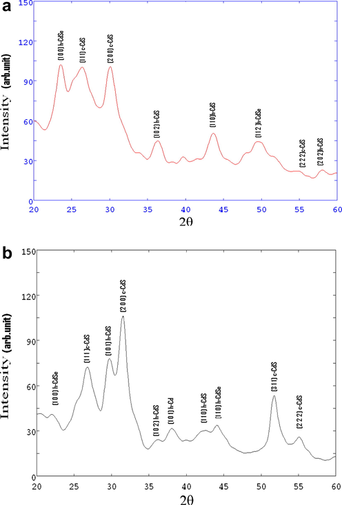
(a) X-ray diffractograms of Cd (S0.7–Se0.3). (b) X-ray diffractograms of Cd (S0.7–Se0.3):CdCl2, La films.
Inter planner spacing (d values)
Intensity
Miller indices (hkl)
Lattice constant
Obs. values (Å)
Rep. values (Å)
Obs. values (Å)
Rep. values (Å)
Obs. values (Å)
Rep. values (Å)
(a) Cd (S0.7–Se0.3) films
3.77
3.72
100
100
(1 0 0)h – CdSe
a = 4.35
4.30
3.37
3.36
100
100
(1 1 1)c – CdS
a = 5.837
5.818
2.96
2.90
99
40
(2 0 0)c – CdS
a = 5.920
5.818
2.35
2.45
44
25
(1 0 2)h – CdS
a = 4.137
4.14
c = 6.31
6.71
2.07
2.06
50
80
(1 1 0)h – CdS
a = 4.137
4.135
1.839
1.833
44.3
50
(1 1 2)h – CdSe
a = 4.35
4.30
c = 7.25
7.02
1.672
1.68
22
10
(2 2 2)c – CdS
a = 5.791
5.818
1.58
1.581
22
7
(2 0 2)h – CdS
a = 4.137
4.135
c = 6.82
6.71
(b) Cd (S0.7–Se0.3):CdCl2 (2 ml), La (8 ml) films
4.06
3.72
40
100
(1 0 0)h – CdSe
a = 4.67
4.30
3.32
3.36
71
100
(1 1 1)c – CdS
a = 5.74
5.818
3.0
3.16
77
100
(1 0 1)h – CdS
a = 4.1
4.135
c = 6.81
6.71
2.83
2.90
100
40
(2 0 0)c – CdS
a = 5.66
5.818
2.47
2.45
24
25
(1 0 2)h – CdS
a = 4.1
4.135
c = 6.79
6.71
2.05
2.06
33
57
(1 1 0)h – CdS
a = 4.1
4.135
6.71
2.16
2.15
30
82
(1 1 0)h – CdSe
a = 4.32
4.30
1.76
1.753
51
60
(3 1 1)c – CdS
a = 5.837
5.818
1.66
1.68
25
10
(2 2 2)c – CdS
a = 5.749
5.818
XRD patterns show diffraction peaks corresponding to CdS and CdSe both. The peak intensities change due to incorporation of La as impurity. CdS is found in both cubic and hexagonal phases, which arise due to difference in arrangement of atomic layers. The possible reason for this rising of cubic and hexagonal phases is atomic arrangements as ABC ABC … and AB AB … (Kittle, 1995). Mixed phases are also found as a result of random stacking of very long period (Lopez et al., 2009).
Langer et al. (1966) reported that a solid solution is a mixture of microcrystalline regions of pure CdSe and CdS, where each micro region is composed of a number of unit cells of each material with the lattice-constant of CdS stressed by surrounding CdSe and vice-versa. Such a model explains uniform shift of absorption edge with composition. These researchers found possibility of solid solution consisting of statistical distribution of CdSe and CdS with respect to their overall concentration. Present investigation witnesses the shift of absorption edge. The average particle size is evaluated using famous Debye Scherer’s Formula (Ubale et al., 2007):
System
Particle size D (nm)
Dislocation density (×1015 lin m−2)
Strain ε (lin−2 m−4)
(Cd (S0.7–Se0.3):CdCl2 (3.00 ml), La (4.00 ml)
4.28
54.61
0.00843
Cd (S0.7–Se0.3):CdCl2 (2.00 ml), La (8.00 ml)
3.39
87.03
0.0106
3.1.2 SEM studies
The SEM micrographs of Cd (S0.7–Se0.3) and Cd (S0.7–Se0.3):CdCl2, La films at a magnification of 5 k are presented in Fig. 2. In both the micrographs, large numbers of clusters comprising of small grains along with some leafy structures are seen. There is some vacant space in fig. (a) between the clusters of non-homogenous spherical grains while fig. (b) shows layered growth along with few fibers. Earlier workers (Bhushan and Shrivastava, 2007) found well developed cabbage structure, which they interpreted in terms of overlapping of different layers formed under continuous growth. Karanjai and Dasgupta (1988) found that CdS grains have greater tendency to coalesce with the increasing concentration of CdCl2. CdCl2 is also known to promote recrystallization of CdS grains (Mukherjee and Bhushan, 2003a,b). The average grain size is calculated using Heyne’s intercept method (Subba Rao et al., 1972) in which instead of estimating the number of grains per unit area, the grains intercepted by a theoretical line on the specimen surface are counted. In the present case, the average particle size is found to lie between 8.3 and 10.7 nm.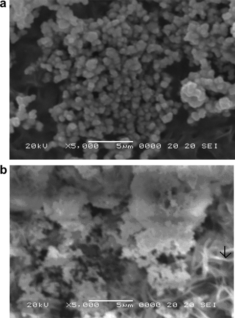
(a) SEM micrographs of Cd (S0.7–Se0.3) film. (b) SEM micrographs of Cd (S0.7–Se0.3):CdCl2, La films.
3.1.3 Optical absorption studies
The study of optical absorption is important in understanding the behavior of semiconductor nano crystals. A fundamental property of semiconductors is band-gap energy separation between the filled valence band and the empty conduction band. Optical excitations of electrons across the band-gap are strongly allowed, producing an abrupt increase in absorption at the wavelength corresponding to the band-gap energy.
Results of optical absorption spectra recorded in the wavelength range 340–660 nm and carried out at RT for pure and doped Cd (S–Se) films are presented in Fig. 3. From these curves it is noticed that absorption is dominant mainly in blue region. As the impurities are added to pure Cd (S0.7–Se0.3) films, absorption peak is blue shifted. This shift is due to the quantization effect according to which the band-gap value increases with the size reduction of crystallites. The band-gap values of these materials determined from the Tauc’s plots (Fig. 4) are found as Cd (S0.7–Se0.3) = 2.16 eV; Cd (S0.7–Se0.3):CdCl2 (2.00 ml) = 2.15 eV; Cd (S0.7–Se0.3):CdCl2 (2.00 ml), La (8.00 ml) = 2.41 eV. The materials of present study are of direct band-gap nature and a slight increase in band-gap value is noticed in La doped sample, which is due to its different ionic radii as compared to that of Cd where it is substituted.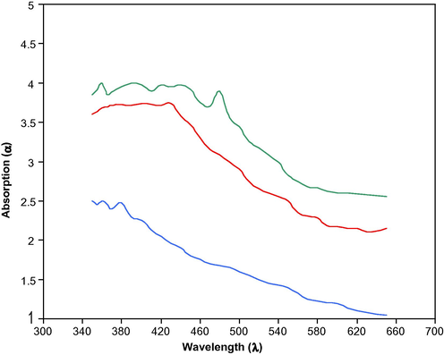
Absorption spectra of different Cd (S0.7–Se0.3) films:
 Cd (S0.7–Se0.3):
 Cd (S0.7–Se0.3). CdCl2 (2 ml),
 Cd (S0.7–Se 0.3) CdCl2 (2 ml), La (8 ml).
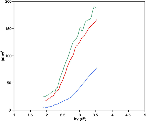
Tauc’s plots of different Cd (S0.7–Se0.3) films:
 Cd (S0.7–Se0.3):
 Cd (S0.7–Se0.3). CdCl2 (2 ml),
 Cd (S0.7–Se0.3) CdCl2 (2 ml), La (8 ml).
The absorption coefficient (α) and the band-gap (Eg) are related by the following expression in direct band-gap materials (Dawar et al., 1990):
3.2 PL spectral studies
The PL spectra of different Cd (S0.7–Se0.3) films at varied concentrations of CdCl2 and La are presented in Fig. 5. PL emission spectrum of CdS peaks at 516 nm (∼2.39 eV), which is quite close to the band-gap (2.43 eV) of pure CdS as observed from the absorption spectrum. Thus, the emission is attributed to edge emission of CdS. Thomas and Hopfield, (1962) correlated this emission to the excitonic transitions involving free excitons. Maximum PL emission is observed for 0.7:0.3 combinations of CdS: CdSe and hence this combination is used for PL studies. In presence of CdCl2, the highest emission is obtained at a volume of 2.00 ml. Therefore, this concentration is used in the presence of impurities.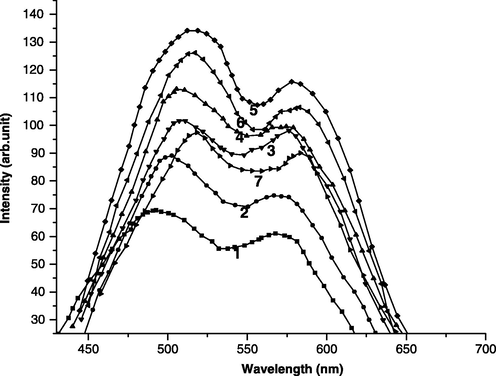
PL emission spectra of different Cd (S0.7–Se0.3) films: (1) Cd (S0.7–Se0.3), (2) Cd (S0.7–Se0.3): CdCl2 (2 ml), (3) Cd (S0.7–Se0.3): CdCl2 (2 ml), La (4 ml), (4) Cd (S0.7–Se0.3): CdCl2 (2 ml), La (6 ml), (5) Cd (S0.7–Se0.3): CdCl2 (2 ml), La (8 ml), (6) Cd (S0.7–Se0.3): CdCl2 (2 ml), La (10 ml), (7) Cd (S0.7–Se0.3): CdCl2 (2 ml), La (12 ml).
The peak positions of different films are listed in Table 3. Cd (S–Se) films with ratio of 0.7:0.3 show two broad emission peaks. The lower wavelength emission is associated to a annihilation of free excitons because of similar excitonic nature of edge emission of CdS and CdSe (Bhushan and Oudhia, 2009). The broadening of this peak is attributed to the localized excitonic state with a broad distribution of energies (Shevel et al., 1987) along with exciton-lattice coupling and scattering. The second peak is found to shift towards higher wavelength with increasing percentage of Se. This emission is associated to donor–accepter transitions formed by incorporations of cations (excess Cd in present case) introducing deep accepter levels (like S vacancies with ionization energy ∼0.03 eV) and that of anions (S or Se in present case) introducing deep accepter levels (Cd vacancies with ionization energy typically ∼1.1 eV for sulphides and ∼0.6 eV for selenides). Bhushan and Pillai (2008), through EDX measurements have already reported that in such preparation excess CdS exists as compared to its counter part. With increasing concentration of La, these peak positions get shifted towards longer wavelength side. This supports that these emissions are not due to direct transitions in energy bands of La.
System
Peak positions (nm)
Intensities
Cd (S0.7–Se0.3)
495, 570
70, 60
Cd (S0.7–Se0.3):CdCl2 (2.00 ml)
504, 573
89, 72
Cd (S0.7–Se0.3):CdCl2 (2.00 ml), La (6.00 ml)
508, 576
102, 98
Cd (S0.7–Se0.3):CdCl2 (2.00 ml), La (8.00 ml)
516, 580
134, 116
Cd (S0.7–Se0.3):CdCl2 (2.00 ml), La (10.00 ml)
515, 581
126, 107
Cd (S0.7–Se0.3):CdCl2 (2.00 ml), La (12.00 ml)
519, 583
97, 91
However, the origin of emission peaks, in presence of La is related to transitions between the excitonic levels of pure Cd (S–Se) and the energy levels due to La, which cause slight shift in emission peaks. Further improvement in peak intensities is also observed in presence of La, which is due to energy transfer from energy levels of La. Improvement in intensities of emission peaks in presence of CdCl2 is due to better crystallization in its presence (Mukherjee and Bhushan, 2003a, b).
4 Conclusions
-
La doped Cd (S0.7–Se0.3):CdCl2 films are prepared through CBD technique, which is a simple and suitable method for obtaining smooth, uniform, high reflecting and strong adherent thin films.
-
Sufficiently intense PL spectra are observed in Cd (S0.7–Se0.3):CdCl2 films prepared on glass substrate at RT. These samples can be used as a PL device.
-
PL emission spectra of chemically deposited Cd (S0.7–Se.0.3), Cd (S0.7–Se0.3):CdCl2, La (8 ml) films consist of two peaks, which are related to the transition between excitonic levels and levels due to La. Thus, La can be preferred as dopant to enhance PL intensity.
-
SEM studies show layered growth of films while XRD patterns exhibit diffraction lines corresponding to CdS, CdSe and Cd.
-
Absorption spectra exhibit direct band-gap nature of material.
Acknowledgements
The authors are thankful to IUE – DAE, Indore for XRD and SEM studies. One of the authors (S.A.) thanks U.G.C., New Delhi for awarding teacher fellowship to her.
References
- Comparative study of performance of CdS, CdSe thin filmCdS-PTh, CdSe-PTh nanocomposite thin films Using SEM-EDXA (Scanning Electron Microscope) and FTIR (Fourier Transform Infrared Spectroscopy) Lat. Am. J. Phys. Educ.. 2010;4(3):603-609.
- [Google Scholar]
- Stability effect in photoconducting studies of some chemically deposited films. Turk. J. Phys.. 2008;32:21-29.
- [Google Scholar]
- Photoconductivity and photoluminescence in chemically deposited films of CdSSe:CdCl2, Ho. Opto-Electro. Rev.. 2009;17(1):30-39.
- [Google Scholar]
- Photoconductivity and photoluminescence in chemically deposited films of (Cd–Zn)S:CdCl2Tb films. Cryst. Res. Technol.. 2008;43(7):762-768.
- [Google Scholar]
- Photoconductive properties of chemically deposited CdS:La films. J. Phys. D: Appl. Phys.. 1990;23:909.
- [Google Scholar]
- Material characterization of chemically deposited photoconducting CdS films. Cryst. Res. Technol.. 1992;27:555-560.
- [Google Scholar]
- Photoconductivity, photovoltaic effect and photoluminescence in chemically deposited films of (Cd0.95–Pb0.05)S:CdCl2, Gd. Opt. Mater.. 2006;28:1334-1340.
- [Google Scholar]
- Nanocrystalline properties of chemically deposited (Cd0.95–Pb0.05)S:CdCl2, Gd/Dy films. Cryst. Res. Technol.. 2007;42(10):983-990.
- [Google Scholar]
- Photoconductivity of chemically deposited lanthanum/neodymium doped (Cd–Pb)S films. Radiat. Eff. Defects Solids. 2001;153(4):367-377.
- [Google Scholar]
- Electro-optical studies in chemically deposited La/Nd doped (Cd–Pb) films. J. Mater. Sci.. 2002;13:581.
- [Google Scholar]
- Photoconducting and photovoltaic studies on some chemically deposited (Cd–Zn)S-@@-(Cd–Pb)S films. J. Mater. Sci.. 2004;39:6303-6309.
- [Google Scholar]
- Photoconductive properties of dip-deposited CdS:Cu, Cl thin films sensitised in situ. J. Phys. D: Appl. Phys.. 1988;21:1769.
- [Google Scholar]
- Introduction of Solid State Physics (seventh ed.). New York: John Willy and Sons; 1995. 18
- Phys. Rev.. 1966;152(2):788.
- Ordered stacking fault arrays in silicon nanowires. Nano Lett.. 2009;9(7):2774-2779.
- [Google Scholar]
- Mater. Chem. Phys.. 2008;163:24.
- Photoconductive properties of some chemically deposited (Cd–Pb)S films. Radiat. Eff. Defects Solids. 2003;158:491-498.
- [Google Scholar]
- Effect of CdCl2 on the photoconductivity of chemically deposited neodymium doped (Cd–Pb)S films. Opt. Mater.. 2003;22(1):51-57.
- [Google Scholar]
- Electrical properties of sintered CdSxSe1−x films. Chalcogenide Lett.. 2008;5(9):181-186.
- [Google Scholar]
- Influence of substrate temperature on the properties of vacuum evaporated InSb films. Cryst. Res. Technol.. 2005;40:573.
- [Google Scholar]
- Picosecond luminescence of excitons localized by disorder in CdSxSe1−x. J. Lumin.. 1987;37:45-50.
- [Google Scholar]
- Structural and optical properties of chemically deposited Cd(S–Se):CdCl2. Sm Films. 2009;32(2):125-133.
- [Google Scholar]
- Experiments in Materials Science. New York: Springer; 1972.
- Optical properties of bound exciton complexes in cadmium sulfide. Phys. Rev.. 1962;128:2135-2148.
- [Google Scholar]
- Size dependent optical characteristics of chemically deposited nanostructured ZnS thin films. Bull. Mater. Sci.. 2007;30(2):147-151.
- [Google Scholar]
- Solid State Commun.. 1999;109:757.
- White electroluminescence from a poly (N-vinylcarbazole) layer doped with CdSe/CdS core-shell quantum dots. Nanotechnology. 2006;17(19):4966.
- [Google Scholar]