

Translate this page into:
Effect of RF and AC powers on morphological, structural, and optical properties of plasma polymerized EDOT thin films
⁎Corresponding author. mjrahman@phy.buet.ac.bd (Mohammad Jellur Rahman)
-
Received: ,
Accepted: ,
This article was originally published by Elsevier and was migrated to Scientific Scholar after the change of Publisher.
Peer review under responsibility of King Saud University.
Abstract
This study focused on the effects of alternating current (AC) and radio frequency (RF) power in the formation of plasma polymerized 3,4-ethylenedioxythiophene (PPEDOT) thin films onto glass substrates. Field emission scanning electron microscopy revealed that thin films produced both in AC and RF conditions exhibited a pristine surface morphology without any pinholes. Fourier transform infrared spectroscopy indicated that the chemical compositions of the PPEDOT films differed from that of the 3,4-ethylenedioxythiophene (EDOT) monomer due to structural rearrangements. The energy band gap values determined from the UV–Vis spectra were approximately 3.68 eV for the samples produced under AC power, while those for the samples produced under RF power were relatively higher, around 3.84 eV. Furthermore, the thin films synthesized using RF power and AC power exhibited significant differences in optical properties, including Urbach energy, extinction coefficient, steepness parameter, refractive index, optical conductivity, and skin depth. The EDOT monomer, PPEDOT and computed PEDOT via Density Functional Theory have been explicitly modeled with the intend to scrutinize the interplay between polymer formation and the modulation of molecular orbital energy levels, calculating band gaps, and molecular vibrations.
Keywords
PPEDOT thin films
Plasma polymerization
Radio frequency
Density functional theory
Optical band gap

1 Introduction
The current trend focusing on organic thin films has attained significant research attention because of their potentiality in modern technologies across various fields due to their unique properties and functionalities. Organic thin films are utilized in electronic devices such as organic field-effect transistors, gas sensors, biosensors, chemical sensors (Choi et al., 2015), barrier coatings, flexible displays, packaging materials, organic light emitting diodes (LEDs), and organic photovoltaics offering a potential solution for renewable energy generation (Liu and Ueda, 2009). Thin films for optoelectronic and photovoltaic applications require high optical transparency and optimal band gap, smooth and defect-free surfaces, high electrical conductivity, stable chemical composition, special optical properties, and mechanical stability.
There are several deposition techniques to prepare organic thin film such as solution-based techniques, spin or spray coating (Li et al., 2021), plasma-enhanced chemical vapor deposition (PECVD) (Bae et al., 2005), electrochemical deposition processing (Gueye et al., 2020), atmospheric plasma deposition (Massines et al., 2005), oxidative type in-situ polymerizations (Kumar et al., 2021). Among these techniques, plasma polymerization stands out as a form of PECVD which is cost-effective and environmentally friendly (Haidar et al., 2022). It also provides desirable features, including faster deposition rates and precise control over the film thickness (Shen and Bell, 1979). The technique typically produces uniform, chemically inert thin films which are mechanically stable and possess unique optoelectronic properties (Çökeliler et al., 2007).
In this study, plasma polymerized 3,4-ethylenedioxythiophene (PPEDOT) thin films have been synthesized using the 3,4-ethylenedioxythiophene (EDOT) as a monomer precursor deposited by a capacitively coupled parallel plate reactor. The plasma glow is generated using alternating current (AC) of 50 Hz and radio frequency (RF) of 13.56 MHz powers. Recently, a thickness-dependent study on structural and optical behavior of PPEDOT thin films, deposited using only AC plasma power, has been published (Sarder et al., 2022). But, in the present study, the effect of AC and RF powers on surface morphology, structural and optical properties of PPEDOT thin films have been presented and finally a comparative investigation is reported. The EDOT monomer is selected for this study because of its advantageous characteristics including high optical transparency, excellent chemical stability, and promising potentials in doped states (Zhang et al., 2021). These attributes make it an attractive material for various applications, particularly in organic photovoltaic technology. EDOT has demonstrated its advanced capabilities and has emerged as a promising material in recent years (Roncali et al., 2005).
Recently, several researchers have used RF power to develop thin films, which has a significant effect on the properties of the resulting thin film. The RF power influences the deposition rate of the films (Michelmore et al., 2013). Higher RF power typically leads to an increased deposition rate, resulting in structural and electrical changes in the deposited films within a given time (Mohamed et al., 2006). Moreover, the optical band gap decreased with increasing rf power, and both the refractive index and extinction coefficient increased observed by a recent study (El-Hossary et al., 2021).
By controlling the RF power, it is possible to achieve films with different thicknesses. The degree of crosslinking and the length of polymer chains in the film can be influenced by RF power. Higher RF power often increases the extent of cross-linking between polymer chains resulting in a denser film structure (Tajima and Komvopoulos, 2007). This can influence the mechanical, thermal, and chemical properties of the film. At higher RF powers plasma species are more and lead to increased fragmentation, surface roughness, and ionization of monomers. These can result in changes in the chemical composition of the film including an increase in the incorporation of reactive functional groups or the generation of more branched structures (Bazaka and Jacob, 2009). RF power also plays a role in determining the electrical properties of PP films. Varying the RF power, it is possible to control the conductivity or resistivity of the film, which are suitable for applications in electronic devices, sensors, or coatings with specific electrical requirements (Agostino et al., 1987). RF-based systems often utilize capacitively coupled plasma reactors, which operate at lower pressures compared to AC-based systems. Lower-pressure environments reduce the likelihood of contaminants from the surrounding atmosphere being incorporated into the thin film during deposition (Sajeev et al., 2006).
Considering the above aspects, AC and RF plasma-based PPEDOT thin films would find suitable applications in thin film technology due to their advantageous chemical and physical properties. Computational calculations have been executed to predict and validate the structural, vibrational, and electronic properties of the EDOT monomer and PPEDOT, complementing and enhancing the interpretation of the experimental results. These investigations have been focused on vibrational modes, the energy levels of the highest occupied molecular orbital (HOMO) and the lowest unoccupied molecular orbital (LUMO), as well as the spectral properties. The purpose of these computational assessments is to validate the outcomes obtained from the experimental results.
Unlike previous studies, the comparative study of AC and RF power in the synthesis of PPEDOT thin films explained the detailed analysis of the structural, chemical, and optical properties of EDOT and PPEDOT thin films, alongside computational modelling of PEDOT, offering new insights into the relationship between polymer formation and modulation of molecular orbital energy levels. This comprehensive approach provides a deeper understanding of the effects of AC and RF power on PPEDOT thin films, contributing to the development of optimized materials for electronic and optoelectronic applications.
2 Experimental details
2.1 Materials
The EDOT (C6H6O2S, purity ≥ 97 %, CAS No. 126213–50-1) monomer used in this study is purchased from Sigma-Aldrich, Germany. The chemical structure of the EDOT is displayed in Fig. 1. The boiling point and molecular weight of this monomer are 193 °C and 142.18 g/mol, respectively. EDOT has been chosen because of its medium boiling points, high conductivity, non-toxic nature (Roncali et al., 2005). Other important properties of this monomer such as density, refractive index, flash point, and storage temperature are 1.34 g/cm3, 1.5765, 104 °C, and 2 − 8 °C, respectively. The glass substrates on which the films were deposited, and the monomer container were of Sail Brand, China, and other necessary equipment were collected from the local market. The rotary pump (Alcatel Vacuum Technology, Model: OME-25-S, United Kingdom) is used for achieving and maintaining the desired vacuum level within the reactor chamber during the glow discharge processes.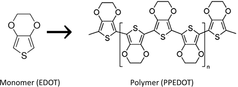
The optimized chemical structure of EDOT and expected PPEDOT polymer structure.
2.2 Methods
The process started with resizing glass substrates using a cutter and cleaning with detergent. Attaining flawless polymer films needed specific cleaning. After 15 min in detergent, slides were rinsed, acetone treated, and ultrasonically cleaned. Remaining impurities were removed by rinsing with deionized water and drying before deposition. The glow discharge plasma setup includes a reaction chamber, electrode system, pumping unit, gauge, power sources, monomer injection, and flow meter as in Fig. 2. In this setup, the plasma glow is generated between two electrodes connected to a capacitively coupled system. The clean glass substrates are placed on the lower electrode. When the pressure in the reactor chamber is reduced to 9.33 Pa, the plasma glow is generated by applying AC (50 Hz) to the electrodes for the preparation of PPEDOT (AC) samples. To prepare the PPEDOT (RF) samples, the input power source is changed as a result a RF generator of 13.56 MHz power is placed to the electrodes.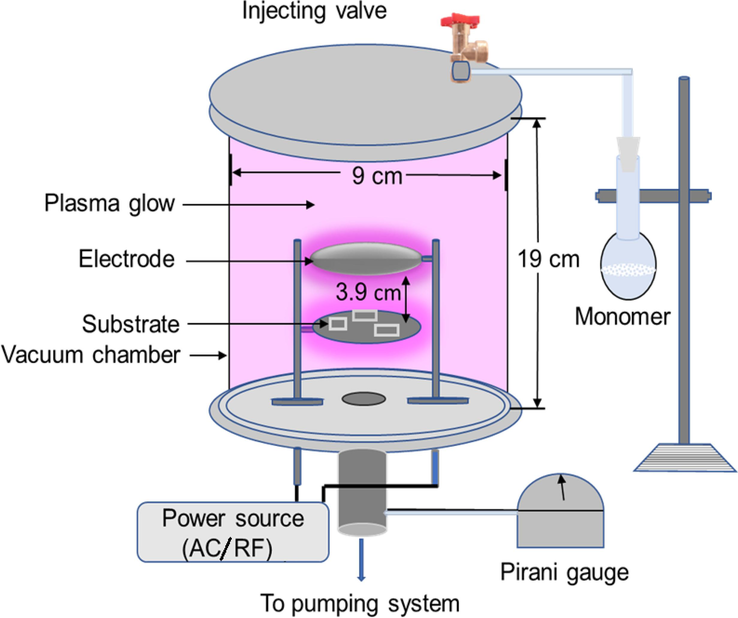
Schematic diagram of the plasma polymerization set-up in the laboratory.
To prevent condensation of EDOT vapor, the monomer tube along with the monomer container is heated to 75 °C using a hairdryer. This enables easy injection of the monomers into the plasma reactor. An injection valve to maintain a stable working pressure of approximately 17.3 Pa during the deposition process controls the monomer flow rate. With a constant input power of around ∼ 37 W for both AC and RF power systems, the monomer molecules begin absorbed and condensed onto the glass substrates. In this study, films deposited for 30 min under both the power systems, were selected for comparison purposes.
The characteristics of a film such as optical properties, and electrical properties are widely dependent on film thickness. Therefore, thickness measurement of the thin film is very important. In this study, the thickness of the deposited films was recorded with the help of the FESEM cross-sectional analyses. It is observed that power source has significant effect on the films thickness produced under same power and for same deposition duration (Mohamed et al., 2019). For the PPEDOT film produced under AC power the thickness (250 nm) is much lower than the film produced under RF power (687 nm) It may happen because of providing current of higher frequency by an RF generator, which facilitates better ionization of the process gas in the plasma-based deposition techniques (Tajima and Komvopoulos, 2007). The increased ionization leads to a higher density of reactive species, which promotes film growth compared to AC. The higher ionization levels in RF plasmas allow more efficient film deposition, which increases the thicknesses (Biederman and Slavínská, 2000). Again, RF plasma enhances the flux of reactive species toward the substrate, allowing for faster film growth. This higher deposition rate enables the preparation of thicker films in a relatively shorter period of fragmentation or etching of monomers (Banu et al., 2018). Therefore, it can be said that the deposition rate of PPEDOT (RF) is higher than PPEDOT (AC) thin films.
2.3 Characterization techniques
Field emission scanning electron microscopy (FESEM) (JEOL JSM 7600F, USA) is used to obtain high-resolution images of the sample to investigate the surface morphological features of the PPEDOT thin films. To mitigate the charging effect that can occur during FESEM imaging, the PPEDOT films were coated with a thin layer of platinum (Pt) using a sputtering coater. A double-beam SIMADZU FTIR-8400 Fourier transform infrared (FTIR) instrument was employed to analyze the bonding characteristics of the PPEDOT films. The FTIR spectra of the samples are recorded, allowing the identification of various types of bond vibrations present in the films. This analysis helps in understanding the chemical composition, structural properties, and the presence of specific functional groups or polymerization degrees within the PPEDOT films. To determine the band gap energy and other optical parameters UV–visible spectra of the deposited PPEDOT thin films were recorded at room temperature using a UV–Vis spectrophotometer (Shimadzu UV-2600, Japan).
2.4 Computational method
Density functional theory (DFT) was employed in this study to complement experimental data and gain deeper insights into the structural and electronic properties of plasma polymerized thin films. DFT allowed for structural optimization, simulation of infrared spectra, and calculation of the HOMO-LUMO gap, providing detailed atomic-level insights and predictive power. These simulations validated experimental results and enhanced our understanding of the material's behavior and properties. All computational simulations within the theoretical framework were conducted utilizing the SCIGRESS software package, version FO 3.5.0 (Hara et al., 2019). Quantum chemistry computations. Specifically, the semi-empirical PW91 generalized gradient approximation (GGA) method was employed to discern the minimum energy geometries of the isolated PPEDOT polymer and the EDOT monomer. Subsequently, the energies pertaining to the molecular orbitals were computed based on the optimized geometrical structures. This approach facilitated an in-depth examination of the impact of polymerization on the energy levels of the molecular orbitals within the PPEDOT. Vibrational transitions were calculated using DGauss, employing the B88-PW91 GGA energy functional and double-zeta valence polarized (DZVP) basis sets at the system’s optimized geometry (Xu and Goddard, 2004). The UV–Vis electronic transitions were meticulously determined employing the ZINDO computational method with INDO/S parameters. This was conducted at a geometry optimized using the DGauss suite of programs, incorporating the B88-PW91 GGA functional and the DZVP basis sets (Li et al., 2021).
3 Results and discussion
3.1 Surface morphology and compositional analyses
The FESEM micrographs of the PPEDOT AC and RF thin films are taken at an accelerating voltage of 5 kV. Fig. 3 shows the top and cross-sectional views of the films prepared on to glass substrates for a 30 min of deposition time. Fig. 3 (a) represents the FESEM images of the as-deposited PPEDOT (AC) and Fig. 3(b) represents that of the RF thin films. The surfaces of the films deposited under AC and RF powers are observed to be smooth, pinhole-free, scratch-less, flawless and homogeneous. Kabir et al. also found similar surface morphology of the PP pyromucic aldehyde films deposited using a capacitively coupled glow discharge system (Kabir et al., 2012). Though input power influences the degree of polymerization, there are no significant changes that can be found between PPEDOT (AC) and PPEDOT (RF) thin films. The cross-sectional view of PPEDOT (AC) and PPEDOT (RF) thin films of thickness 250 nm and 687 nm, respectively are presented in Fig. 3(c) and (d), where it can be observed that the films are smooth at the cross-section and are deposited uniformly on to the glass substrate. Again, it is also obvious that the thin films hold exceedingly small grains, and the deposited layer shows a smooth view.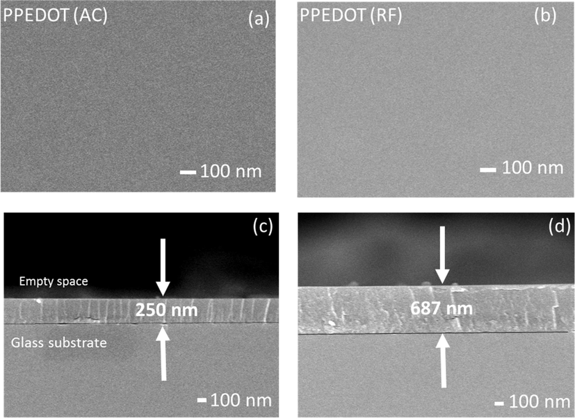
Top view (a, b) and cross-sectional view (c, d) of the FESEM images of (a, c) PPEDOT(AC) and (b, d) PPEDOT(RF) thin films.
This smooth surface is crucial for efficient light emission, charge transport, and electrical performance of the devices (Sheikh et al., 2023). The smooth surfaces offer versatility and can be tailored to specific requirements by selecting appropriate materials and deposition techniques. Smooth organic thin films can also be employed in surface modification to alter the surface properties of the substrates (Nemani et al., 2018). Including all the above advantages, these smooth PPEDOT films may enhance the hydrophobicity or hydrophilicity of surfaces, control surface energy, and provide lubricity or low-friction properties. It can be used as a biocompatible coating to improve the compatibility of medical devices with biological tissues (Martin, 2015).
3.2 Energy dispersive X-ray analysis
In thin film technology energy dispersive X-ray (EDX) is studied for identifying contaminants, investigating elemental composition changes, examining elemental segregation, studying crystal structures, analyzing geological specimens, assessing coatings, and more. The EDX spectra, collected from the unit attached to the FESEM, have been taken to identify and quantify elements in the samples indicating atomic percentages of the constituents of PPEDOT thin films (Pachauri et al., 2015). The EDX spectra of the as-deposited PPEDOT thin films are shown in Fig. 4 for the films fabricated by AC and RF plasma. The monomer used in the study consists of carbon (C), oxygen (O), sulfur (S), and hydrogen (H), however the presence of H cannot be detected in PPEDOT due to the limitations of EDX analysis (Yasmin et al., 2024). In addition to the basic elements of EDOT, PPEDOT thin films also contain some other elements such as silicon (Si), magnesium (Mg), sodium (Na), aluminum (Al), calcium (Ca). Of these Si, Ca, and Mg are may came from the glass substrates and other may be came during the polymerization process or from the surrounding atmosphere when the samples were taken out of the reactor chamber. Table 1 provides the atomic percentage (at %) of the constituent elements present in the PPEDOT thin films. The presence of platinum (Pt) can be attributed to the fact that the films were coated with a thin layer of Pt using a sputtering coater while taking the FESEM images to obtain accurate and detailed images of the film’s structure and features without the interference of artifacts caused by charge accumulation (Pachauri et al., 2015).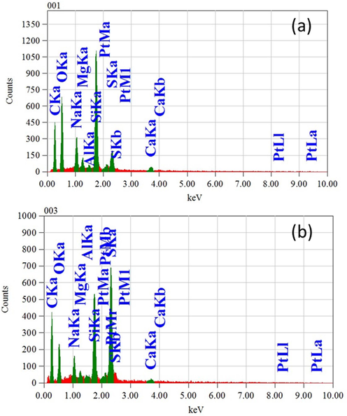
EDX spectra of the (a) PPEDOT (AC), and (b) PPEDOT (RF) thin films.
Element detected
EDOT (at %) (calculated)
Contents (at %)
PPEDOT (AC)
PPEDOT (RF)
C
37.61
58.23
67.72
O
21.42
22.94
13.81
S
10.71
10.49
10.26
H
30.26
Not detected
Not detected
Si
−
2.75
5.95
Mg
−
1.02
0.44
Na
−
3.35
1.47
Al
−
0.23
0.04
Ca
−
0.96
0.26
Pt
−
0.03
0.05
Total
100.00
100.00
100.00
In this comparative study, it is noted that the at % of C in the RF PPEDOT is greater than that of AC PPEDOT. It may happen that RF plasma can increase the reactivity of carbon-containing precursors, facilitating the incorporation of more C atoms into the growing film (Rahman and Bhuiyan, 2013). The energetic species in the plasma can break the chemical bonds of the precursor molecules leading to the release of C species that can contribute to the composition of the film. RF power has also enhanced the overall deposition rate of the film and can result in a higher C content in the films (Li et al., 2017).
In some cases, RF plasma can induce polymerization reactions, where the precursor molecules undergo cross-linking or polymer chain formation. These reactions can also generate larger molecular structures with higher C content, leading to an increase in the C element observed in the film. Additionally, overall composition of the PPEDOT (RF) films may depend on the choice of EDOT precursor and its relative concentrations (Casado et al., 2016). On the other hand, the at% of O is decreased and other elements changes randomly. It is a common effect in EDX undergoing decomposition or degradation over the time due to environmental factors such as temperature, humidity, or exposure to light (Lakshmi et al., 2010). This decomposition can result in changes in elements-containing functional groups, leading to a decrease in the C content of the film (Laforgue and Robitaille, 2010). Again, this EDOT monomer contains a volatile C-based compound, it may evaporate from the film over the period causing a reduction in the C content. The PPEDOT can be sensitive to contamination from the two different power sources, handling procedures, or exposure to ambient conditions. It is also important to consider the possibility of analytical artifacts during the analysis process, which may have an important effect on changing the elemental quantity (Liu et al., 2017).
3.3 Structural analyses: FTIR spectroscopy
FTIR spectra of both the EDOT monomer and the as-deposited PPEDOT films (including AC and RF-computed thin films) are shown in Fig. 5 at room temperature in transmittance mode covering a range from 500 to 3500 cm−1. Comparing the FTIR spectra of PPEDOT with the monomer EDOT reveals a noticeable decrease in absorption band intensity in PPEDOT. This decrease is linked to molecular vibration changes during plasma polymerization. Table 2 lists key absorption peaks and their possible identifications for reference. In the spectrum of the EDOT, all the significant absorption bands have been identified, and some of them closely resemble with the peaks observed in PEDOT (AC) films, details of which was reported in our pervious study (Sarder et al., 2022).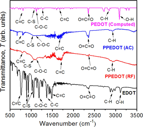
FTIR spectra of the EDOT monomer, as-deposited PPEDOT (AC), PPEDOT (RF), and PEDOT (computed) thin films.
Assignment
Wavenumber (cm−1)
EDOT
PPEDOT
AC
RF
Computed
C=C
755
781
762
786
C−S ring stretching
831, 886, 1023
1035
1048
1031
C−O−C stretching
1366
1376
1388
1388
C−C stretching
1471
−
−
1468
C=C stretching
1584
1747
1741
1720
C−H bending
1951
−
−
−
O=C=O stretching
2356
2343
2346
2351
C−H stretching
2934
2926
2930
2895
O−H stretching
3113
−
−
3117
In the FTIR spectra of PPEDOT (AC) and PPEDOT (RF) thin films, the stretching band of C=C shifted very slightly towards lower wavenumber. Upon comparing FTIR spectra of the PPEDOT films to the spectrum of EDOT it is observed that the intensity of the absorption peaks in PPEDOT is weakened. This confirms the occurrence of monomer fragmentation during the polymer synthesis in the plasma reactor chamber. In the PPEDOT spectra, some absorption bands which are present in the monomer spectrum are absent, while new peaks emerge as a result of polymerization (Kiristi et al., 2015).
However, the characteristic absorption bands associated with the ethylenedioxy groups and the thiophene backbone are still present in PPEDOT. The absorption peaks around 1035 cm−1 in the PPEDOT (AC) and PPEDOT (RF) spectra, which correspond to the C-S stretching vibrations of the thiophene backbone, closely resemble those observed in the monomer spectrum. This confirms the presence of sulfur atoms in the polymer structure. The absorption peaks around 1377 and 1384 cm−1 indicate the presence of C−O−C stretching vibrations in the ethylenedioxy groups, contributing to the solubility and processability of PEDOT (Lim et al., 2021). This may be attributed to the conjugation within the chemical structure (Kiristi et al., 2015). The absorption peaks observed around 1620 and 1623 cm−1, suggest the presence of conjugation, specifically C=C stretching vibrations, in the PPEDOT spectra. The appearance of peaks at 2343, 2347, and 2351 cm−1 corresponds to the O=C=O stretching mode, primarily resulting from the stretching of the benzene ring (Sarder et al., 2022). In EDOT monomer, the O−H stretching absorption band is found around 3113 cm−1, but this spectrum was not identified in AC and RF PPEDOT. It may be happened due to form some new covalent bonds in the PPEDOT backbone consumed during the polymerization (Lim et al., 2021). These investigations provide evidence that the chemical structure undergoes modification or change during plasma polymerization. The fragmentation of EDOT during polymerization is supported by the transformation of multiple bands into a single broadband, as observed in the spectra of PPEDOT compared to EDOT. As a result of the formation of PPEDOT, the thin films exhibit an aromatic ring structure with C-S side groups. The peaks corresponding to C−O−C stretching in PPEDOT are slightly shifted to higher wavenumbers, varying with AC and RF powers. This shift may be attributed to an increase in cross-linking within the PPEDOT thin films at higher frequencies.
By comparing the above spectra of AC and RF PPEDOT thin films, differences in the intensity corresponding to absorption peaks position are observed that indicate species interactions during film growth. Though RF films show comparatively strong absorption peaks to AC films, but the variations in bonding configurations between AC and RF PPEDOT indicate the presence of unwanted by-products or chemical contaminants (Abessolo et al., 2018) and the structure of PPEDOT departs to some range from that of the monomer structure. Operating at higher power densities compared to AC plasma leads to variations in energy input effects on the film’s molecular structure (Michelmore et al., 2013). For the majority of the vibrational modes, the experimental data of the wavenumbers for EDOT and PPEDOT coincide closely with the computed values for PEDOT. This alignment substantiates the reliability of the experimental findings. Computational data from DFT calculations are a useful tool for predicting these values, and it validates the experimental methodologies used to obtain these results.
3.4 UV–visible spectroscopic analyses
The optical absorption feature of the PPEDOT thin films as-synthesized with AC and RF power were investigated to analyze several optical parameters including transmittance, optical band gap, Urbach energy, etc., which were studied in the wavelength range of 300 − 800 nm at room temperature. The variation of absorbance and transmittance corresponding to AC and RF PPEDOT films and simulated results are shown in Fig. 6(a) and 6(b), respectively. In the UV–visible region (200 − 800 nm), the absorbance of AC and RF PPEDOT demonstrates a marked increase, peaking at approximately 270 nm, which is in perfect alignment with the simulated results for PEDOT. Furthermore, it is observed that the absorption of PEDOT polymers, both in experimental and simulated cases, shows an increase when compared to the monomer EDOT. Subsequently, the absorbance decreases rapidly up to around 375 nm. Beyond this point, the value of the absorbance spectra changes very slowly and becomes nearly constant at a wavelength of approximately 550 nm.
Spectral distribution of (a) the absorbance of the PPEDOT (AC) and PPEDOT (RF) thin films, (b) the transmittance, T (%) and Reflectance, R of the thin films as a function of wavelength.
It is noticed that all the absorption peaks for AC and RF films are placed in the UV region, where the wavelength corresponding to absorbance peaks transferred slightly from 250 nm to 268 nm, which perfectly aligns with the peak absorbance of computed one (268.32 nm). It may be assigned to the persistence of conjugation in the PPEDOT thin film (Kim et al., 2019). Another observation is that the intensity of the absorption peak does not change significantly in the visible region, and becomes almost zero at higher wavelength, which suggests that the PPEDOT films are very transparent in this region. Maximum absorbance happened in the UV regions, which may be due to the electronic transitions occurring within the organic molecules, or conjugated systems in the film. The position and intensity of absorption peaks can indicate the presence of chromophores or functional groups within the organic material (Chowdhury and Bhuiyan, 2000).
The optical transmittance graphs of the PPEDOT thin films are plotted in Fig. 6 (b) where in the lower wavelength region of 350 − 550 nm the transmittance of the RF sample is slightly lower than those of the AC sample, but it shifts quickly to 86 % transmittance corresponding to 575 − 735 nm wavelengths. As the thicker films tend to exhibit lower transmittance due to increased light absorption and scattering, PPEDOT (AC) film showed greater transmittance compared to PPEDOT (RF) films. High transmittance in the visible region allows the PPEDOT thin films to remain optically clear, enabling the integration of PEDOT coatings without compromising the visibility or functionality of underlying components (Sheikh et al., 2023). Optical transmittance directly affects device efficiency in optoelectronic devices utilizing PPEDOT thin films, such as solar cells or LEDs (Sarder et al., 2022).
The band gap energy, Eg, is expressed as the optical transitions in the electronic band structure of the PPEDOT thin films, which is estimated by the Tauc relation (Mallick, 2023; Hameed et al., 2022) αhν = C (hν – Eg)n Here, C, the Tauc parameter represents the proportionality factor, hν indicates the photon energy and n exhibits the nature of the optical transition. Generally, EDOT and PEDOT show a direct bandgap (Sarder et al., 2022). Fig. 7(a) for PPEDOT (AC) and PPEDOT (RF) thin films, shows a slight difference in the value of the band gap energy. The PPEDOT (RF) exhibits the highest optical band gap as calculated as 3.84 eV, whereas AC samples show 3.68 eV, because of the development of excess crosslinking within the bulk of the material because of the impact of RF plasma on the surface during the deposition process (Sajeev et al., 2006).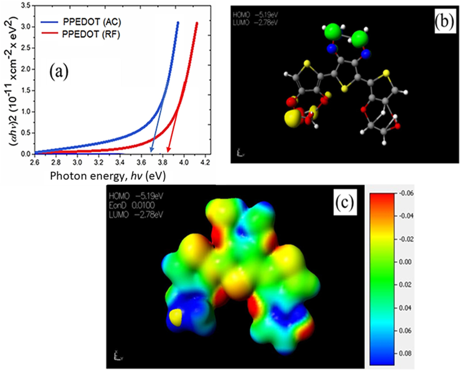
Band gap energy of the PPEDOT thin films (a) deposited in AC and RF powers, (b) HOMO-LUMO of PEDOT computed through DFT, (c) electrostatic energy of PEDOT computed through DFT.
The band gap of PEDOT calculated through DFT was determined to be 2.51 eV. This difference in value of Eg was obtained because the thickness considered for the computed PEDOT is high, which exhibited a bulk-like behavior. This trend further supports the validity of the experimental results, validating the comparison with the calculated PEDOT. The molecular electrostatic potential (MEP) was calculated to predict the reactive sites for potential electrophilic and nucleophilic attacks on the optimized structures, as depicted in Fig. 7(c). In the MEP map, the red color indicates areas of maximum negative potential, which are favorable sites for electrophilic attack. Conversely, the blue color represents areas of maximum positive potential, which are favorable sites for nucleophilic attack. The green color corresponds to regions with zero potential. The color grading in MEP simultaneously displays the information regarding molecular size, shape, the distribution of positive, negative, and neutral electrostatic potentials. Analysis of the MEP map reveals that the regions with a negative potential coincide with electronegative atoms, particularly oxygen atoms, while the regions with a positive potential are located over hydrogen atoms (Kanchana et al., 2023).
In the low photon energy region, the Urbach empirical rule that describes spectral dependence of α on hν is given by Eq. (1) (Akther et al., 2023);
Here. Urbach energy, Eu, originating from defect states or disorders of the PPEDOT (AC and RF) films and is measured from the slope of the straight-line portion of the curve lnα versus hν as shown in Fig. 8.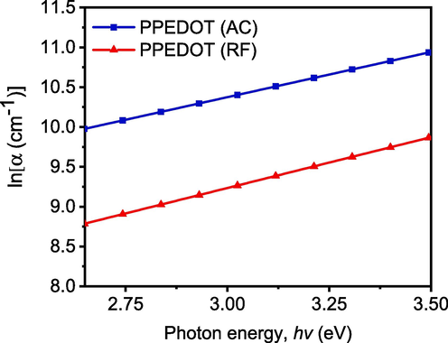
The lnα vs hν plots for the as deposited PPEDOT (AC) and PPEDOT (RF) thin films.
The value of for the as-deposited PPEDOT thin films are calculated from the inverse gradients of the lnα versus hν plots, as shown in Fig. 8. The observed values of are 0.881 eV and 0.783 eV for AC and RF PPEDOT thin films, respectively. The more value of for PPEDOT (AC) film indicates the increase of disorder-induced states or structural defects and also suggests the presence that can impact the film’s electrical and optical properties by the introduction of localized states within the forbidden energy gap (Nasrin et al., 2018; Shaban et al., 2020). Higher Urbach energy implies a broader tail in the absorption spectrum, extending to lower energies (longer wavelengths). The ranged around 0.781 − 0.883 eV for organic thin film suggesting that the absorption tail extends into the near-infrared region. This broadening of the absorption spectrum can have implications for the utilization of PPEDOT thin films in optoelectronic devices, as it may limit the range of wavelengths that can be efficiently absorbed (Chantana and Kawano, 2020).
The steepness parameter, σs, which is correlated to , can be estimated as = (Solaymani et al., 2021). Here, is the Boltzmann constant and T being the absolute temperature. The values are determined by taking T=298 K and it is seen that value of RF film (0.033) is slightly greater than AC film (0.029). A lower steepness parameter indicates a less efficient charge transport in the PPEDOT thin film due to poor molecular ordering, higher resistance, or increased scattering of charge carriers. The σs value also represents the rate at which the current changes with respect to the voltage broadening of the optical absorption edge in consequence of electron–phonon or exciton-phonon interactions (Chowdhury and Bhuiyan, 2000). As a result, the AC films may exhibit lower and slower charge transport properties compared to RF films (Dalouji et al., 2022). Comparing above values between AC and RF plasma, it can be said that PPEDOT (RF) has allowed improved injection/extraction of charges compared to PPEDOT (AC) films.
The extinction coefficient, k =
, quantifies the attenuation of a light beam as it passes through the films (Banu et al., 2018). It is observed from Fig. 9(a) that k drops with λ in both cases of PPEDOT thin films due to the occurrence of electron transport across the mobility gap (Kabir et al., 2020). The RF sample shows a greater k value compared to the AC sample, which indicates RF plasma treatment results in higher absorption of light compared to AC plasma treatment for PPEDOT thin films. As RF plasma typically operates at higher frequencies as well as higher plasma density and a higher degree of surface modification, it results in higher absorption of light (Xu and Goddard, 2004).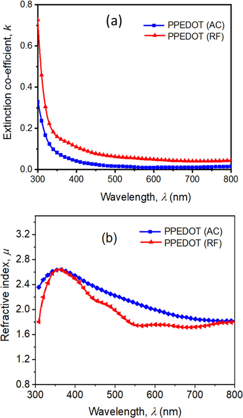
The variation of extinction coefficient (a), and the refractive index (b) against wavelength for the as-deposited PPEDOT thin films (AC and RF).
The refractive index, μ, of the PPEDOT films is measured using Fresnel’s formula (Rahman and Bhuiyan, 2013) presented in Eq. (2) where the μ values for both films (AC and RF) reach as high as 2.64 corresponding 400 nm wavelength region, above which μ decreased. In higher wavelength regions as shown in Fig. 9(b), PPEDOT (RF) films shows less μ value compared to PPEDOT (AC).
However, the values of μ change very slightly in higher wavelength region with the change in the power source, which may occur due to change in the interactions between photons and electrons in the films depending on the plasma power. The value of μ when is > 1.5 for both cases, therefore the PPEDOT is referred to high refractive index polymer (Rahman and Bhuiyan, 2013).
Optical conductivity (
) measurements contribute to the comprehensive characterization of PPEDOT thin films that conduct electricity under varying electromagnetic frequencies including conductivity and resistivity. By analyzing optical conductivity, it can assess the quality of PPEDOT thin films produced through different fabrication methods and correlate with device performance metrics like efficiency, response time, and stability. The variation of
with the wavelength of the films is measured by using the Eq. (3) (Nasrin et al., 2022).
Here, c is the velocity of light. The changes in
are plotted against λ in Fig. 10 (a). It is clearly seen that
of the AC films are higher than RF films. The maximum values of
are noted in the lower wavelength region (345 to 365 nm). For all the deposited PPEDOT thin films, the value of
tends to decrease and approach towards zero in the higher wavelengths, specifically above 600 nm. The value of
for both samples in these ranges may affect the absorption characteristics, including α and the energy of the absorbed light (Sarder et al., 2022).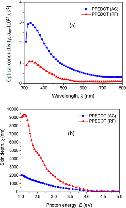
Variation of (a) optical conductivity,
, and (b) skin depth, χ, with wavelength for the AC and RF PPEDOT thin films.
The skin depth, χ, determines the essence of the contract to an incident wave of light and the electrons in the PPEDOT thin films. Here, χ = that decreases monotonically with increasing photon energy and changes with the different power sources of the films as shown in Fig. 10 (b).
The χ in PPEDOT thin films influences the absorption characteristics of light within the material. As the hν changes, the χ provides information about the depth at which light is absorbed. Understanding the variation of χ with hν, the range of wavelengths at which PPEDOT thin films effectively absorb light can be identified and these types of films have more applications in photodetectors or solar cells (Volman et al., 2014).
All the results obtained from various experimental investigations of AC and RF PPEDOT thin films are summarized in Table 3. No significant changes are found in the films’ quality in terms of surface morphological, elemental and structural properties, but it shows slight changes in terms of the films’ thicknesses and optical behavior.
Property
PPEDOT (AC)
PPEDOT (RF)
Film thickness
250 nm
687 nm
Surface morphology
Smooth and pinhole-free
Smooth and pinhole-free
Elemental constituent
Pure
Pure
Functional group
New bands created compared to EDOT monomer
Some broad and strong bands created compared to AC plasma
Band gap energy
3.68 eV
3.84 eV
Urbach energy
0.78 eV
0.88 eV
Steepness parameter
0.033
0.029
Refractive index
2.64
2.61
From this comparative study, firstly noticed that, RF power source can produce thicker films within a shorter time compared to an AC power source in spite of maintaining all parameters constant. As thickness is an important significant parameter in thin film technology, where the films containing low thickness have more applications because of their lightweight and interesting physio-chemical properties. So, it can be noted that, RF power can produce a thin film within a shorter duration compared to AC power. Again, in many cases, some properties like higher Eu, and lower indicate RF films offers advantages in terms of uniformity, control, and compatibility, making it a preferred option for preparing organic thin films compared to AC. The RF films exhibit the highest optical band gap and sharp strong IR spectra compared to AC films because of excess crosslinking within the bulk of the material The MEP analysis reveals the regions with a negative potential coincide of oxygen atoms, while the regions with a positive potential are located over hydrogen atoms. In this work, various characterizations such as morphological, structural and optical properties of as-deposited AC and RF PPEDOT thin films are performed. Apart from this, thickness dependent RF samples can be prepared and studied different properties of the PPEDOT thin films to get better understanding. The PPEDOT thin films for both cases (AC and RF) have been determined to exhibit physical, chemical, and optical stability. The results obtained from the fundamental characterizations indicate that these films hold significant potential for applications in the fields of organo-electronics, photovoltaics, and thermoelectric.
4 Conclusions
High-quality PPEDOT thin films with smooth, uniform, and pinhole-free surfaces were successfully synthesized using both AC and RF powers. The deposition rate of the films under RF power was observed to be higher compared to the films produced under AC powered plasma. AC or RF power do not have significant influence on surface morphological and elemental composition of the films. From the structural investigations, it is identified that there are some new broad and sharp peaks in PPEDOT (RF) films due to the variation of new functional groups and effects of higher frequencies input power. There is a remarkable alignment in the vibrational modes across the EDOT, PPEDOT (AC), and PPEDOT (RF) demonstrating the reliability of the computational predictions. The UV–visible spectra analysis describes that the absorbance plots are overlapping but other optical properties show slight changes. The experimental band gap energies observed are proximate and reach up to 3.80 eV. In contrast, the computational band gap is calculated to be around 2.51 eV, a value that is based on considerations of the bulk properties of PPEDOT. The band Eg remains almost nearby and up to 3.80. Again, other optical properties such as the Eu, , k, μ, , and χ show slight differences but these ranges indicate almost similar characteristics for both the samples. As the PPEDOT thin films exhibit a smooth surface, adjustable optical properties, and stable structural rearrangements, meeting key requirements for optoelectronic and photovoltaic applications. These properties make them suitable for efficient light interaction and charge transport in devices like solar cells, LEDs, and photodetectors.
CRediT authorship contribution statement
Md. Juel Sarder: Writing – original draft, Investigation, Formal analysis, Data curation, Conceptualization. Md. Saddam Sheikh: Writing – review & editing, Validation, Investigation, Data curation, Formal analysis, Writing – original draft. Md. Abdul Momin: Visualization, Validation, Investigation, Formal analysis. A.H. Bhuiyan: Writing – review & editing, Visualization, Validation. Mohammad Jellur Rahman: Writing – review & editing, Visualization, Validation, Supervision, Conceptualization.
Acknowledgments
The authors would like to express gratitude for the financial support provided by the Committee for Advanced Studies and Research (CASR) of the Bangladesh University of Engineering and Technology (BUET), Dhaka, Bangladesh. They would also like to acknowledge the Nanotechnology Research Laboratory of the Department of Physics, BUET, for providing access to their UV-visible spectroscopy and valuable experimental data.
Declaration of competing interest
The authors declare that they have no known competing financial interests or personal relationships that could have appeared to influence the work reported in this paper.
References
- Atmospheric plasma oxidative polymerization of ethylene dioxythiophene (EDOT) for the large-scale preparation of highly transparent conducting thin films. Plasma Process Polym.. 2018;15(4):1700172.
- [CrossRef] [Google Scholar]
- Mechanisms of deposition and etching of thin films of plasma‐polymerized fluorinated monomers in radio frequency discharges fed with C2F6‐H2 and C2F6‐O2 mixtures. J. Appl. Phys.. 1987;61:2754-2762.
- [CrossRef] [Google Scholar]
- Insights into the structural and optical features of plasma polymerized N, N, 3, 5 tetramethylaniline-2,6-diethylaniline thin films. Opt. Mater.. 2023;144:114278
- [CrossRef] [Google Scholar]
- Bae, I.S., Cho, S.B., Lee, Kim, Y., and Boo, J.H., 2005. Growth of plasma-polymerized thin films by PECVD method and study on their surface and optical characteristics. Surf. Coat. Technol., 193, 142–146. doi: 10.1016/j.surfcoat.2004.07.022.
- Characterization of structural and optical properties of plasma polymerized diethanolamine thin films. Adv. Polym. Technol.. 2018;37:3084-3094.
- [CrossRef] [Google Scholar]
- Synthesis of radio frequency plasma polymerized non-synthetic Terpinen-4-ol thin films. Mater. Lett.. 2009;63:1594-1597.
- [CrossRef] [Google Scholar]
- Plasma polymer films and their future prospects. Surf. Coat. Technol.. 2000;125:371-376.
- [CrossRef] [Google Scholar]
- PEDOT radical polymer with synergetic redox and electrical properties. ACS Macro Lett.. 2016;5(1):59-64.
- [CrossRef] [Google Scholar]
- Impact of Urbach energy on open-circuit voltage deficit of thin-film solar cells. Sol. Energy Mater Sol. Cells. 2020;210:110502
- [CrossRef] [Google Scholar]
- Choi, K., Nam, S., Lee, Y., Lee, M., Jang, J., Jin Kim, Jin Jeong, S., Y., Kim, H., Bae, S., Yoo, J.B., Cho, S.M., Choi, J.B., Kyoon Chung, H. Ahn, J.H. Eon Park, C., Hee Hong, B., 2015. Reduced water vapor transmission rate of graphene gas barrier films for flexible organic field-effect transistors. ACS Publ. 9, 5818–5824. doi: 10.1021/acsnano.5b01161.
- An investigation of the optical properties of plasma-polymerized diphenyl thin films. Thin Solid Films. 2000;360:69-74.
- [CrossRef] [Google Scholar]
- Modification of glass fibers to improve reinforcement: A plasma polymerization technique. Dent. Mater.. 2007;23(3):335-342.
- [CrossRef] [Google Scholar]
- Skin depth, optical density, electron-phonon interaction, steepness parameter, band tail width, carriers transitions and dissipation factors in Cu-Co bilayer films. Mech. Adv. Mater. Struct.. 2022;29:6634-6647.
- [CrossRef] [Google Scholar]
- ZnO thin films prepared by RF plasma chemical vapour transport for self-cleaning and transparent conducting coatings. Bull. Mater. Sci.. 2021;44:1-13.
- [CrossRef] [Google Scholar]
- Progress in understanding structure and transport properties of PEDOT-based materials: A critical review. Prog. Mater. Sci.. 2020;108:100616
- [CrossRef] [Google Scholar]
- Surface-active plasma-polymerized nanoparticles for multifunctional diagnostic, targeting, and therapeutic probes. ACS Appl. Nano Mater.. 2022;5:17576-17591.
- [CrossRef] [Google Scholar]
- Vanadium-doped CuO: Insight into structural, optical, electrical, terahertz, and full-spectrum photocatalytic properties. Opt. Mater.. 2022;133:113029
- [CrossRef] [Google Scholar]
- Hara, A., Kazimierczak, H., A. B.-A. of M., 2019, Effect of different organic additives on surface morphology and microstructure of Zn-Mo coatings electrodeposited from citrate baths. Arch. Metall. Mater., 64, 207–220. doi: 10.24425/amm.2019.126240.
- Structural and optical properties of plasma polymerized pyromucic aldehyde thin films. Int. J. Mech. Mechatron. Eng.. 2012;12:30-34.
- [Google Scholar]
- Heat treatment effect on the structural, morphological, and optical properties of plasma polymerized furan-2-carbaldehyde thin films. Results Phys.. 2020;16:103014
- [CrossRef] [Google Scholar]
- Kanchana, S., Kaviya, T., Rajkumar, 2023, Computational investigation of solvent interaction (TD-DFT, MEP, HOMO-LUMO), wavefunction studies and molecular docking studies of 3-(1-(3-(5-((1-methylpiperidin-4-yl) methoxy) pyrimidin-2-yl) benzyl)-6-oxo-1, 6-dihydropyridazin-3-yl) benzonitrile. J. Chem. Phys. 7, 100263. doi: 10.1016/j.chphi.2023.100263.
- Polymerization of 3, 4-Ethylenedioxythiophene and Pyrrole by plasma enhanced chemical vapor deposition (PECVD) for conductive thin film with tunable energy bandgap. Macromol. Res.. 2019;27:243-249.
- [CrossRef] [Google Scholar]
- A comparison study of microwave and radio frequency plasma polymerized PEDOT thin films. J. Macromol. Sci. Part A Pure Appl. Chem.. 2015;52:124-129.
- [CrossRef] [Google Scholar]
- Thickness dependent microwave attenuation behaviour of Ferrite-PANI composites and embedded composite-fabrics prepared by in situ polymerization. AIP Adv.. 2021;11:015106
- [CrossRef] [Google Scholar]
- Production of conductive PEDOT nanofibers by the combination of electrospinning and vapor-phase polymerization. J. Biol. Macromol.. 2010;43:4194-4200.
- [CrossRef] [Google Scholar]
- Synthesis and characterization of thin films of poly (3-methyl thiophene) by rf-plasma polymerization. Mater. Lett.. 2010;64:1672-1673.
- [CrossRef] [Google Scholar]
- Recent advancement of emerging nano copper-based printable flexible hybrid electronics. ACS Nano.. 2021;15:6211-6232.
- [CrossRef] [Google Scholar]
- Optimized pseudopotentials and basis sets for semiempirical density functional theory for electrocatalysis applications. J. Phys. Chem. Lett.. 2021;12:10304-10309.
- [CrossRef] [Google Scholar]
- Fabrication and structural characterization of plasma polymerized polypyrrole thin film. Surf. Coat. Technol.. 2017;320:206-212.
- [CrossRef] [Google Scholar]
- Improvement of electrochemical properties of poly(3,4-ethylene dioxythiophene) (PEDOT) thin film by UV irradiation. J. Nanosci. Nanotechnol.. 2021;21:4638-4643.
- [CrossRef] [Google Scholar]
- Plasma polymerization of poly(3,4-ethylenedioxyethene) films: The influence of plasma gas phase chemistry. J. Vac. Sci. Technol. A. 2017;35:021302
- [CrossRef] [Google Scholar]
- High refractive index polymers: Fundamental research and practical applications. J. Mater. Chem.. 2009;19:8907-8919.
- [CrossRef] [Google Scholar]
- Mallick, P. Fundamentals of Molecular Spectroscopy. (2023).
- Molecular design, synthesis, and characterization of conjugated polymers for interfacing electronic biomedical devices with living tissue. Mrs Commun.. 2015;5(2):131-153.
- [CrossRef] [Google Scholar]
- Atmospheric pressure plasma deposition of thin films by Townsend dielectric barrier discharge. Surf. Coat. Technol.. 2005;5–6:1855-1861.
- [CrossRef] [Google Scholar]
- Defining plasma polymerization: New insight into what we should be measuring. ACS Appl. Mater. Interfaces. 2013;5:5387-5391.
- [CrossRef] [Google Scholar]
- Effect of rf plasma nitriding time on electrical and optical properties of ZnO thin films. J. Phys. Chem. Solids. 2006;67:2351-2357.
- [CrossRef] [Google Scholar]
- Study of the effects of both film thickness and annealing time on CuxSyOz thin films for the possibility of usage as solar control coatings. Appl. Phys. A Mater. Sci. Process.. 2019;125:1-10.
- [CrossRef] [Google Scholar]
- Morphological, elemental, and optical characterization of plasma polymerized n-butyl methacrylate thin films. Appl. Phys. A. 2018;124:391.
- [CrossRef] [Google Scholar]
- Thickness dependent thermal and optical properties of plasma polymerized N-benzylaniline thin films. Mol. Cryst. Liq. Cryst.. 2022;738:50-66.
- [CrossRef] [Google Scholar]
- Surface modification of polymers: methods and applications. Adv. Mater.. 2018;5(24):1801247.
- [CrossRef] [Google Scholar]
- A standard characterization methodology for respirable coal mine dust using SEM-EDX. Resour.. 2015;4:939-957.
- [CrossRef] [Google Scholar]
- Structural and optical properties of plasma polymerized o-methoxyaniline thin films. Thin Solid Films. 2013;534:132-136.
- [CrossRef] [Google Scholar]
- 3, 4-Ethylenedioxythiophene (EDOT) as a versatile building block for advanced functional π-conjugated systems. J. Mater. Chem.. 2005;15:1589-1610.
- [CrossRef] [Google Scholar]
- Sajeev, U.S., Joseph Mathai, C. S., Saravanan, Ashokan, R.R., Venkatachalam, S. Anantharaman, M.R., 2006. On the optical and electrical properties of RF and AC plasma polymerized aniline thin films. Bull. Mater. Sci. 29, 159–163. doi: 10.1007/BF02704609.
- Sarder, M.J., M.M., Hasan, Bhuiyan, A.H., Rahman, M.J., 2022. Thickness dependence of structural and optical behavior of plasma polymerized 3,4-ethylenedioxythiophene thin films, Opt. Mater., 134, 113170. doi: 10.1016/j.optmat.2022.113170.
- The influence of substrate temperatures and thickness on optical and electrical conductivity of CuIn(Se0.25S0.75)2. J. Inorg. Organomet. Polym. Mater.. 2020;30:1360-1368.
- [CrossRef] [Google Scholar]
- Direct current conduction mechanism in the methyl acrylate – vinyl acetate composite thin films. Sci. Rep.. 2023;1–11
- [CrossRef] [Google Scholar]
- Structural and optical behaviours of methyl acrylate-vinyl acetate composite thin films synthesized under dynamic low-pressure plasma. Heliyon. 2023;9:e18524.
- [CrossRef] [Google Scholar]
- Shen, M. and Bell, A.T., 1979. A review of recent advances in plasma polymerization. https://pubs.acs.org/doi/abs/10.1021/bk-1979-0108.ch001.
- Optical properties and surface dynamics analyses of homojunction and hetrojunction Q/ITO/ZnO/NZO and Q/ITO/ZnO/NiO thin films. Results Phys.. 2021;29:104679
- [CrossRef] [Google Scholar]
- Dependence of nanomechanical modification of polymers on plasma-induced cross-linking. J. Appl. Phys.. 2007;101:014307
- [CrossRef] [Google Scholar]
- Radio-frequency-transparent, electrically conductive graphene nanoribbon thin films as deicing heating layers. ACS Publ.. 2014;6:298-304.
- [CrossRef] [Google Scholar]
- The X3LYP extended density functional for accurate descriptions of nonbond interactions, spin states, and thermochemical properties. Proc. Natl. Acad. Sci. U. S. A.. 2004;101:2673-2677.
- [CrossRef] [Google Scholar]
- A comprehensive study on structural and optical properties of zinc selenide/poly ortho-methoxyaniline hybrid thin films deposited by chemical bath deposition and plasma polymerization techniques. Arab. J. Chem.. 2024;17
- [CrossRef] [Google Scholar]
- Nanostructured PEDOT coatings for electrode-neuron integration. ACS Appl. Bio Mater.. 2021;4:5556-5565.
- [CrossRef] [Google Scholar]