

Translate this page into:
Nanostructured pyramidal black silicon with ultra-low reflectance and high passivation
⁎Corresponding author at: School of Opto-Electronic and Communication Engineering, Xiamen University of Technology, Xiamen 361024, China. sylien@xmut.edu.cn (Shui-Yang Lien)
-
Received: ,
Accepted: ,
This article was originally published by Elsevier and was migrated to Scientific Scholar after the change of Publisher.
Peer review under responsibility of King Saud University.
Abstract
In this study, nanostructured pyramidal black silicon is prepared by metal assisted chemical etching method, in which the silver nitrate (AgNO3) is used as the metal catalyst. Effects of the concentration of AgNO3 on passivation and optical properties of the black silicon are investigated. The experimental results show that at the AgNO3 concentration of 0.03 M, the nanostructure length is about 300 nm, and the reflectance of the black silicon with a stack of silicon nitride (SiNx) and aluminum oxide (Al2O3) is 0.8%, which is comparable to that of the conventional black silicon with micrometer-long nanowires. In addition, an acceptably low surface recombination rate of 42 cm/s can be obtained. Plasma chemical vapor deposited SiNx is deposited well on the top of nanostructures of black silicon, but shows poor coverage at the bottom region. Spatial atomic layer deposited Al2O3 can conformally cover the nanostructures with high passivation quality. Simulation result indicates an improvement of 5.5% of conversion efficiency for the nanostructured pyramidal black silicon solar cell compared to industrial silicon solar cell. The short nanostructured pyramidal surface with low reflectance and high passivation is expected to be helpful for black silicon technology applied to photovoltaic applications.
Keywords
Black silicon
Passivation
Reflectance
Solar cell
Metal assisted chemical etching

1 Introduction
Flat silicon having a reflection of 30–40% of the incident light across a broad spectrum severely limits the efficiency and photosensitivity of photo-electronic devices. To decrease the costs a reduction in silicon absorber thickness demands improved light trapping concepts. Alkaline etching is a common way for single-crystalline silicon (c-Si) solar cells to create pyramidal surfaces, reducing the reflectance of c-Si to about 13–15%. Numerous studies have reported that black silicon has much lower reflection losses than conventionally flat or textured c-Si with simple antireflective coatings (Kroll et al., 2012; Hsu et al., 2014; Liu et al., 2014; Lv et al., 2018; Tan et al., 2019; Toor et al., 2016a, 2016b). The best results of black silicon utilize expensive approaches such as femtosecond laser, leading to challenges to scale up (Sarnet et al., 2008). Scaling is essential for photovoltaic applications as large area of solar cells are needed to generate power for sustainable global energy supply (Pearce, 2002). Among different techniques for fabrication of black silicon nanostructures (Cichoszewski et al., 2013), metal-assisted chemical etching (MACE) is one of the most significant methods owing to its simplicity, low cost and large-area capability (Oh et al., 2012; Chen et al., 2019; Noor et al., 2019; Rahman et al., 2017; Toor et al., 2016b; Chartier et al., 2008). In MACE process, noble metals are previously deposited on silicon to inject holes to the valence band of the silicon substrate, catalyzing oxidation of silicon (Huang et al., 2011; Es et al., 2016). The usually used noble metals are silver, platinum, gold and copper, deposited by sputtering (Huang et al., 2011; Li and Bohn, 2000), evaporation (Koynov et al., 2006), electroless or electrochemical displacement (Bastide et al., 2009; Yae et al., 2003). Gold and platinum are relatively expensive, whereas the etching rate of copper-catalyzed MACE process is low. Silver nitrate (AgNO3) is the most widely used catalyst for black silicon synthesis. The metal can be a continuous layer or separated particles depending on the deposition method. After metal deposition, a hydrogen fluoride (HF)-contained solution is used for silicon dissolution, leading to randomly distributed nanostructures. It has been reported that regular nanowire arrays can be achieved by using a mask (Han et al., 2014; Li et al., 2016). Although a theoretical model of MACE etching has been established for both spatially distributed (Rahman and Boden, 2017) and continuous (Geyer et al., 2012) metal catalysis on silicon, the existing works are mostly based on flat silicon substrates. The required length of the nanostructures is in micrometer level in order to have a very low reflectance of 1% or less (Ma et al., 2018; Repo et al., 2013; Abdulkadir et al., 2019; Vinzons et al., 2017). However, long nanowires in turn mean a high surface area and a large amount of dangling bonds, which increases the difficulties of passivation of silicon. Moreover, sharp and long nanowires are unfavorable for photovoltaic device fabrication especially for doping and thin film deposition. These problems are one of the reasons limiting the conversion efficiency of black silicon solar cells, although the low reflectance is reached. To our best knowledge, black silicon with nanostructures shorter than 400 nm with very low reflectance and satisfactorily high passivation is rarely reported.
In this study, nanostructured pyramidal surfaces of black silicon are prepared by MACE process and passivated by a stack of silicon nitride (SiNx) and aluminum oxide (Al2O3). The MACE process is performed on previously textured pyramidal silicon, instead of planar silicon. Effects of the concentration of the metal catalyst on optical and passivation properties of silicon surface are investigated. Finally, performance of the nanostructured pyramidal black silicon solar cells is evaluated, and compared to that with the industrial standard texture structures. The preparation of black silicon on the pyramidal silicon surfaces mainly has two advantages. The first is that the size of the nanostructures for reaching a very low reflectance is shorter than that prepared on planar silicon surfaces. Secondly, the short nanostructures are easier to be passivated as compared to the long nanostructures, which often suffer from the poor coverage of passivation layers. Although an additional wet-etching process is needed, the two-step wet-etching process still demonstrates high potential in the applications where the ultra-low reflectance and high passivation are both required.
2 Material and methods
P-type (1 0 0) Czochralski c-Si polished silicon wafers with a resistivity of 1–10 Ω-cm and a thickness of 200 ± 20 µm were used as a starting substrate. The wafers were cleaned sequentially with acetone, alcohol, and deionized water at room temperature in an ultrasonic cleaning bath. Unlike the conventional MACE process starting with a planar silicon wafer, the cleaned wafers were immersed in acid solution containing 20 wt% KOH and 3 wt% isopropyl alcohol (IPA) at 80 °C for 40 min to remove saw damage, and to create micrometer-sized pyramids on the wafer surface. The black silicon was fabricated by using MACE process, in which the pyramidal wafers were etched in a solution consisting of AgNO3 and 3 M HF at 50 °C for 3 min, followed by a dip in HNO3 to remove the silver particles. The concentration of the AgNO3 was varied from 0.015 to 0.075 M to investigate its effect on properties of the black silicon. The black silicon wafers after the MACE process were cleaned by standard Radio Corporation America process (Kern and Puotinen, 1970), followed by a dip in HF. To passivate the black silicon, a 15 nm-thick Al2O3 layer was deposited by using spatial atomic layer deposition (s-ALD) with trimethylaluminum (TMA) and H2O as metal source and oxidant, respectively. The s-ALD system consisted of a H2O/TMA/H2O injector and a substrate holder moving back and forth with a speed of 150 mm/s under the injector. The gap between the substrate and injector was 1 mm. The nitrogen gas was used as the carrier gas, and also as the curtain to separate the TMA and H2O to avoid gas phase chemical vapor deposition reaction. The bubbler temperature was 17.5 °C for TMA and 25 °C for H2O. The substrate temperature was kept to 135 °C. The growth rate of the s-ALD Al2O3 was 1.7 Å/cycle. The SiNx antireflective layer with a thickness of 50 nm was deposited using 13.56 MHz inductively-coupled plasma chemical vapor deposition (ICPCVD) with a gas mixture of tetramethylsilane (TMS) and ammonia (NH3). The substrate temperature was 120 °C, and the deposition pressure was 5 mTorr. After SiNx/Al2O3 deposition, the samples were annealed in air at 450 °C to activate passivation. Detailed parameters for the wet etching, s-ALD Al2O3 and ICPCVD SiNx are summarized in Table 1. For the characterization, the reflectance spectra of the black silicon were measured using a spectrometer in the spectral region from 380 to 1000 nm. The thickness of the films was measured by an alpha-step profilometer (D-500, KLA-Tencor, USA). The minority carrier lifetime of the samples was obtained by a lifetime tester (WCT-120, Sinton, CO, USA). The cross-sectional images of the samples were observed by a scanning electron microscopy (SEM, JSM-7800F, JEOL, Tokyo, Japan) and a transmission electron microscopy (TEM, JEM2100, JEOL, Tokyo, Japan).
1st wet etching process
Parameter
Value
Solution temperature (°C)
80
Time (min)
40
KOH concentration (wt.%)
20
2nd wet etching process
Parameter
Value
Solution temperature (°C)
50
Time (min)
3
AgNO3 concentration (M)
0.015–0.075
ALD-Al2O3 thin film deposition
Parameter
Value
Substrate temperature (°C)
135
H2O carry gas flow rate (sccm)
400
H2O dilute gas flow rate (sccm)
4000
TMA carry gas flow rate (sccm)
200
TMA dilute gas flow rate (sccm)
2000
Thickness (nm)
15
ICPCVD-SiNx thin film deposition
Parameter
Value
Substrate temperature (°C)
120
Power (W)
1200
Pressure (mTorr)
5
TMS flow rate (sccm)
35
NH3 flow rate (sccm)
25
Thickness (nm)
50
3 Results and discussion
Fig. 1 shows a schematic diagram of the passivated black silicon at different stages. As shown in Fig. 1a, the pyramidal surface is formed after KOH/IPA etching process. The silicon etching reaction can be expressed by
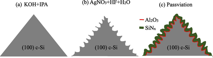
Schematic diagrams of the wet etching processes (a) step 1: KOH etching forming pyramids and (b) step 2: MACE etching forming nanostructures. (c) SiNx/Al2O3 passivation stacked layer on nanostructured pyramidal surface.
The addition of the IPA to KOH lowers the {1 0 0}:{1 1 1} etching-rate ratio, but reduces convex-corner undercutting and smooths the etched surface. Fig. 1b shows the black silicon structure after the MACE process, involving the following chemical reactions
When the Ag+ ions are contact to silicon surface, they reduce to Ag0 with injecting a hole to silicon. The oxidation of silicon occurs, and then dissolved by HF in the form of SiF62−, leading to the Ag particles down into the wafer. The nanostructures are thus produced on the sidewalls of the pyramids. The MACE etching rate is about half compared to that of the planar silicon. Fig. 1c shows the SiNx/Al2O3 passivation layer deposited on the nanostructured pyramids. The deposition quality at the bottom and tip of the high aspect ratio structures is important for achieving low surface recombination rate as the films generally hardly well-cover on those sites. As it will be shown later, the required length of the nanostructures on pyramids for reaching 1% reflectance is much shorter than starting MACE on a planar wafer.
Fig. 2 shows the SEM images of the black silicon with various AgNO3 concentrations. As shown in Fig. 2a, a typical pyramidal surface is observed for the sample with KOH etching alone. The size and uniformity of the pyramids are randomly distributed and can affect the reflectance. Usually, the average pyramidal size ranges from 1 to 9 µm with corresponding reflectance varied between 13 and 15% (Barrio et al., 2012; Manea et al., 2005; Xi et al., 2003). During the wet anisotropic etching process of (1 0 0) silicon, four (1 1 1) sidewalls are exposed to form square-based pyramids with a facet tilt angle of 54° in an ideal process (Hamel and Chibani, 2010; Xi et al., 2014). The tilt angle in this study is slightly smaller. For a practical, non-ideal wet etching process, a slightly smaller tilt angle is normally observed (Baker‐Finch and McIntosh, 2013). In Fig. 2b, the AgNO3 concentration of 0.015 M roughens the pyramidal surface, but does not lead to a spiked surface. This is due to the insufficient Ag concentration. As the concentration increases to 0.03 M shown in Fig. 2c, slice-like nanostructures are tremendously developed on the sidewalls of pyramids. A similar nanostructured surface except for the less density of the slices is observed at the concentration of 0.045 M (Fig. 2d). A transition from slice-like to spike-like nanostructures occurs at the concentration of 0.06 M as shown in Fig. 2e. The spike-like structure is presumably regarded as a degeneration of the slice-like structures as a consequence of the increasing AgNO3 concentration. A higher AgNO3 concentration results in an enhancement of Ag nucleation, which enlarges the size of the Ag particles and thus shortens the space between two neighboring Ag particles. In addition, the HF is harder to diffuse through the Ag/Si interface to remove the silicon oxide compared to the case of a low AgNO3 concentration. This leads to a lower etching rate and a reduced height of the nanostructures at the concentrations of 0.045 and 0.06 M. No nanostructures can be observed at 0.075 M as shown in Fig. 2f, indicating the excessive AgNO3 concentration.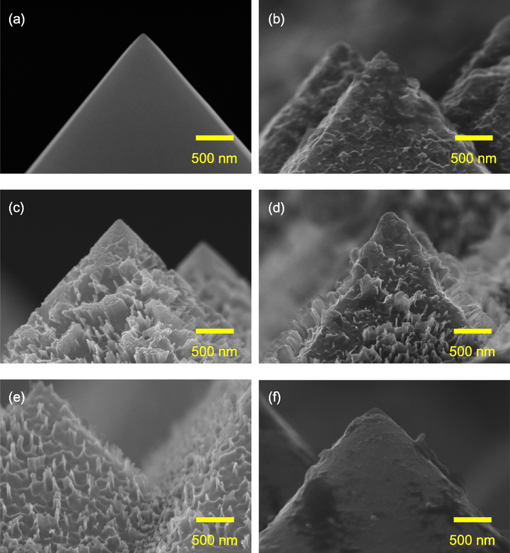
SEM images of black silicon with the AgNO3 concentration of (a) 0 (original), (b) 0.015, (c) 0.03, (d) 0.045, (e) 0.06, and (f) 0.075 M.
Fig. 3 shows the SEM images of the black silicon with a SiNx/Al2O3 passivation stacked layer. The passivation stack can be well-deposited on the sample without MACE process as shown in Fig. 3a. The SiNx/Al2O3 stack has been demonstrated to be one of the best candidates to passivate silicon mainly due to chemical passivation from strong Si—O coordination and hydrogenation at the Si/Al2O3 interface (Dingemans et al., 2010; Naumann, et al., 2012). In addition, field-effect passivation resulting from fixed negative charge inside Al2O3 improves passivation of p-type silicon by repelling minority carriers from surfaces (Hoex et al., 2008). For black silicon, the coverage of the passivation layer on the nanostructures is critical especially at the bottom and top regions. From Fig. 3b–e, it can be seen that the top of the nanostructures is round, indicating that the passivation stack can be deposited regardless on spike- or slice-like structures.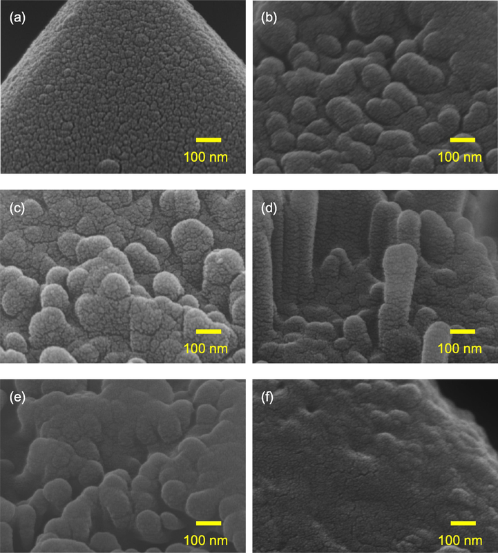
SEM images of SiNx/Al2O3-passivated black silicon with the AgNO3 concentration of (a) 0 (original), (b) 0.015, (c) 0.03, (d) 0.045, (e) 0.06, and (f) 0.075 M.
Fig. 4a shows the reflectance spectra of the pyramidal silicon and the black silicon with different AgNO3 concentration. The reflectance curve of the pyramidal silicon is the highest, which ranges from 15 to 29%. The curves is the lowest when the AgNO3 concentration is 0.03 M, and then increases when the concentration further increases. Fig. 4b shows the reflectance spectra of the black silicon with SiNx/Al2O3 passivation. The reflectance decreases for all the samples compared to before passivation as the intermediate refractive indices of the SiNx and Al2O3 between air and silicon leads to antireflection. The sample with pyramidal silicon demonstrates a typical curve with a minimum at a specific wavelength. There is still about 15–20% reflectance at 400 nm and 5–10% at 1000 nm. All the passivated black silicon samples show a reduction of reflectance in the whole investigated wavelength region. The lowest reflectance is at 0.045 M. The average reflectance values over 400–1000 µm are shown in Fig. 4c. The minimum average reflectance is 5.14% at 0.045 M before passivation deposition, and is 0.8% at 0.03 M after the deposition. The AgNO3 concentration of 0.075 M leads to the highest reflectance. This is due to that the nanostructures are removed from the surface, and the pyramidal structure is also damaged as shown in the SEM image.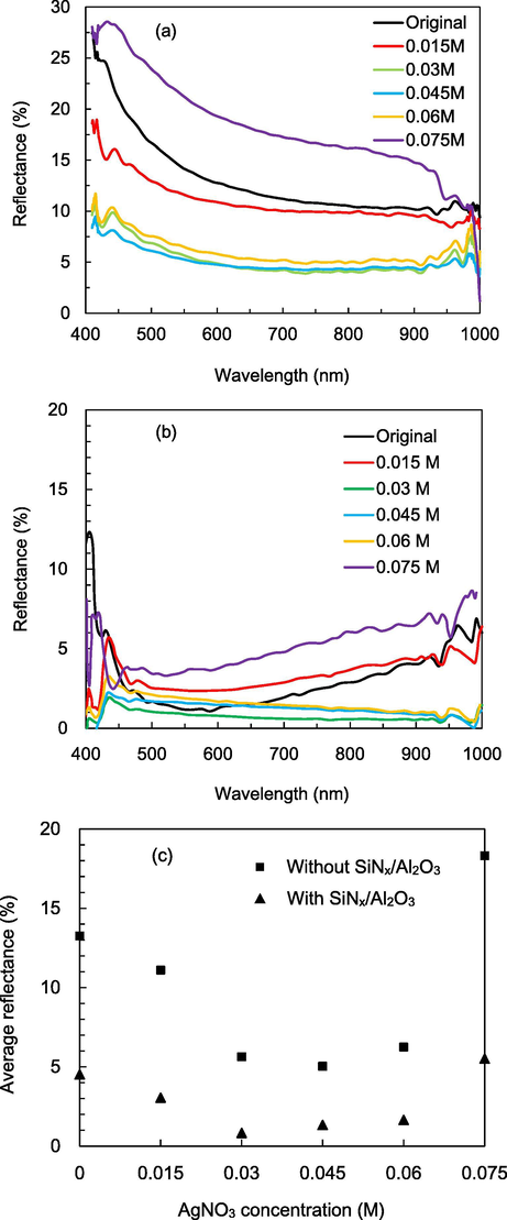
Reflectance spectra of black silicon (a) before and (b) after SiNx/Al2O3 passivation. (c) Average reflectance over 400–1000 nm for black silicon before and after passivation.
Fig. 5a and b shows the injection-level dependent minority carrier lifetime for the black silicon with various AgNO3 concentrations before and after SiNx/Al2O3 passivation, respectively. The lifetime values at 1 × 1015 cm−3 are shown in Fig. 5c. Without passivation, the lifetime values are around 8–20 µs. The black silicon samples have lower lifetimes than pyramidal one due to generation of the defects during MACE process. With passivation, the pyramidal silicon has the highest lifetime of 250 µs, corresponding to a surface recombination rate of 34 cm/s. The lifetime decreases from 217 to 195 µs when the AgNO3 concentration increases from 0.015 to 0.045 M. A drop in lifetime is observed at 0.06 M. The spike-like structures have a higher aspect ratio than sliced-like structures, and thus are more difficult to be passivated. The passivation on the sample with the AgNO3 concentration of 0.075 M leads to the lowest lifetime of 106 µs.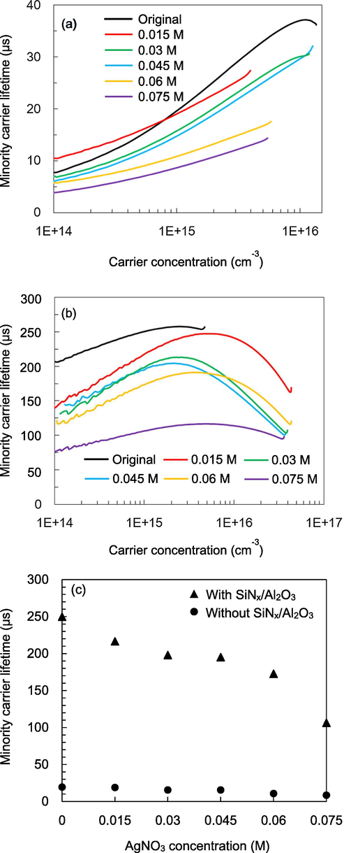
Injection-level dependent minority carrier lifetime of black silicon (a) before and (b) after SiNx/Al2O3 passivation. (c) Minority carrier lifetime at the carrier concentration of 1015 cm−3 for black silicon before and after passivation.
The black silicon with 0.03 M AgNO3 concentration and SiNx/Al2O3 passivation stack has the lowest reflectance, and its cross-sectional SEM images are shown in Fig. 6a. A higher resolution image is shown in Fig. 6b. The nanostructures on the sidewalls of the pyramid are clearly seen. The height of the nanostructures is estimated to be 300 nm or less. It is worthy to point out that in the traditional MACE process, which starts on planar wafers, the required height of the nanowires is twice or even more compared to that in this work to reach a reflectance around 1% (Ma et al., 2018; Repo et al., 2013). However, the passivation quality is compromised as the films are hardly coated well on the sharp and long nanostructures. This problem leads to the black silicon solar cells without conversion efficiency improvement although the absorption of light is enhanced. Reduction in the nanostructure height can improve the passivation layer deposition. Another advantage of the shorter nanostructures is in the aspect of the diffusion process for fabricating a p-n junction. It is known that the junction depth is around 0.5–1 µm for c-Si solar cells (Cheon et al., 2018; Lee et al., 2017; Shen et al., 2014). However, long nanostructures result in a deep junction depth. The emitter is usually regarded as a dead layer as the carriers generated in this region will almost recombine before reaching to the junction (Christesen et al., 2012). In particular, compared to a flat surface, the long spikes of black silicon lead to a higher doping concentration at the surface (Pasanen et al., 2018), which increases the surface recombination rate. A low blue spectral response is expected for c-Si solar cells with a deep and high recombination emitter. Black silicon with short nanostructures could be helpful to diminish these adverse effects.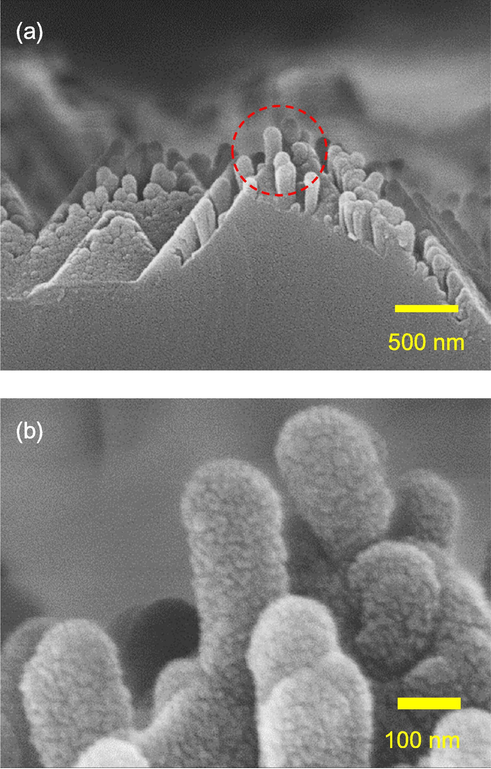
Cross-sectional SEM images of black silicon with the AgNO3 concentration of 0.03 M.
To further investigate the coverage of the passivation layer, cross-sectional images of the black silicon with 0.03 M AgNO3 concentration and SiNx/Al2O3 passivation layer are shown in Fig. 7. It can be seen from Fig. 7a that the thicknesses of SiNx and Al2O3 layer are around 50 and 20 nm, respectively. It can be seen that SiNx covers well on the sidewalls of pyramids. However, some light grey-color regions appear between the nanostructures, indicating that the films are not filled. Fig. 7b shows a higher resolution TEM image of the top region of a black silicon nanostructure. It can be seen that both Al2O3 and SiNx can deposit well on the tip. Fig. 7c shows the bottom between two nanostructures. The labels 1, 2 and 3 correspond to black silicon structures, Al2O3 and SiNx, respectively. Highly conformal deposition of s-ALD Al2O3 is observed. In contrast, an apparent thickness variation along the black silicon structure is observed. The SiNx thickness is less than 10 nm at the bottom of the nanostructure. The SiNx does not present in the region between two nanostructures. This result suggests that the s-ALD is helpful for passivation of black silicon, while the traditional PECVD technique alone might not be adequate to obtain high passivation quality due to the poor coverage.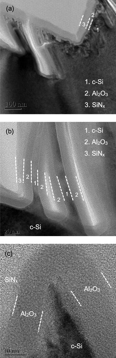
Cross-sectional TEM images of black silicon with the AgNO3 concentration of 0.03 M.
The photovoltaic performance such as open-circuit voltage (Voc), short-circuit current density (Jsc), fill factor (FF) and conversion efficiency (η) of the black silicon solar cells with different AgNO3 concentration and with SiNx/Al2O3 passivation are simulated by PC1D (version 6.2). The minimum set of input parameters is summarized in Table 2. The cell structure is a typical passivated emitter and rear contact cell, and the texturing in this work affects the front surface reflectance and front surface recombination rate. The metal contacts and interfaces are assumed to be ideal. The simulation result is shown in Table 3. For comparison, the industrial standard texturization and passivation are shown as a reference, in which a SiNx single layer is used for passivating the pyramidal silicon. The simulation result indicates that Voc of the reference cell is 664.3 mV. The pyramidal silicon with the SiNx/Al2O3 passivation shows the highest Voc of 678.3 mV. The Voc decreases from 676.8 to 670.4 mV when the AgNO3 concentration increases from 0.015 to 0.075 M. For the Jsc, due to the lowest reflectance, the cell with the AgNO3 concentration of 0.03 M shows the best Jsc of 40.4 mA/cm2, which is significantly higher than the reference cell is 39.3 mA/cm2. The FF is around 0.83 for all the cells. Overall, compared to industrial standard configuration, the best conversion efficiency is 22.9%, which is higher than 21.7% of the reference cell.
Parameter
Value
Exterior front reflectance (%)
Variable
Exterior rear reflectance (%)
0
Internal optical reflectance (%)
90
Wafer thickness (μm)
170
P-type background doping (cm−3)
1016
N-type doping (cm−3)
1019
Front surface recombination (cm/s)
Variable
Rear surface recombination (cm/s)
20
Bulk recombination lifetime (μs)
250
Concentration (M)
Voc (mV)
Jsc (mA/cm2)
FF
η (%)
Industry
664.3
39.3
0.83
21.7
Original
678.3
39.4
0.83
22.2
0.015
676.8
39.9
0.83
22.4
0.03
675.7
40.8
0.83
22.9
0.045
674.1
40.6
0.83
22.7
0.06
671.9
40.4
0.83
22.5
0.075
670.4
38.9
0.83
21.6
4 Conclusions
Low reflectance and high passivation can be achieved by fabricating nanostructured pyramids on silicon surfaces by MACE process and a stack of s-ALD Al2O3 and ICPCVD SiNx. Varying the AgNO3 concentration leads to a transformation from slice to spike-like nanostructures, which are removed at the concentration of 0.075 M. The nanostructured pyramidal black silicon at 0.03 M with a SiNx/Al2O3 stack demonstrates the ultra-low reflectance of 0.8%, which is comparable to that of the black silicon with micrometer-level nanowires. Moreover, an acceptably low surface recombination of 42 cm/s is obtained. The ALD shows a high conformal deposition on black silicon. The ICPCVD SiNx covers well on the top of the nanostructures, but has a poor coverage at the bottom and between two nanostructures. The simulation shows a conversion efficiency improvement by 5.5% can be reached as compared to that with current industrial texturization. In addition to the low reflectance and high passivation, the short-nanostructured black silicon proposed in this work should be easier to be applied to subsequent solar cell fabrication processes due to the surface morphology.
Acknowledgements
This work was sponsored by the Science and Technology Project of Xiamen (No. 3502Z20183054) and the Science and Technology Program of the Educational Office of Fujian Province (No. JT180432).
Declaration of Competing Interest
The authors declare that they have no known competing financial interests or personal relationships that could have appeared to influence the work reported in this paper.
References
- Optimization of etching time for broadband absorption enhancement in black silicon fabricated by one-step electroless silver-assisted wet chemical etching. Optik. 2019;187:74-80.
- [CrossRef] [Google Scholar]
- Reflection distributions of textured monocrystalline silicon: implications for silicon solar cells. Prog. Photovolt. Res. Appl.. 2013;21:960-971.
- [CrossRef] [Google Scholar]
- Optimisation of NaOH texturisation process of silicon wafers for heterojunction solar-cells applications. Sol. Energy. 2012;86:845-854.
- [CrossRef] [Google Scholar]
- Chemical etching of Si by Ag nanocatalysts in HF-H2O2: application to multicrystalline Si solar cell texturisation. Phys. Status Solidi C. 2009;6:1536-1540.
- [CrossRef] [Google Scholar]
- Metal-assisted chemical etching of silicon in HF– H2O2. Electrochim. Acta. 2008;53:5509-5516.
- [CrossRef] [Google Scholar]
- Enhanced blue responses in nanostructured Si solar cells by shallow doping. J. Phys. D Appl. Phys.. 2018;51:125102.
- [CrossRef] [Google Scholar]
- MACE nano-texture process applicable for both single- and multi-crystalline diamond-wire sawn Si solar cells. Sol. Energy Mater. Sol. Cells. 2019;191:1-8.
- [CrossRef] [Google Scholar]
- Design principles for photovoltaic devices based on Si nanowires with axial or radial p–n junctions. Nano Lett.. 2012;12:6024-6029.
- [CrossRef] [Google Scholar]
- Role of catalyst concentration on metal assisted chemical etching of silicon. Electrochim. Acta. 2013;109:333-339.
- [CrossRef] [Google Scholar]
- Hydrogen induced passivation of Si interfaces by Al2O3 films and SiO2/Al2O3 stacks. Appl. Phys. Lett.. 2010;97:2-5.
- [CrossRef] [Google Scholar]
- An alternative metal-assisted etching route for texturing silicon wafers for solar cell applications. IEEE J. Photovoltaics. 2016;6:440-446.
- [CrossRef] [Google Scholar]
- Model for the mass transport during metal-assisted chemical etching with contiguous metal films as catalysts. J. Phys. Chem. C. 2012;116:13446-13451.
- [CrossRef] [Google Scholar]
- Characterization of texture surface for solar cells. J. Appl. Sci.. 2010;10:231-234.
- [CrossRef] [Google Scholar]
- Metal-assisted chemical etching of silicon and nanotechnology applications. Nano Today. 2014;9:271-304.
- [CrossRef] [Google Scholar]
- On the c-Si surface passivation mechanism by the negative-charge-dielectric Al2O3. J. Appl. Phys.. 2008;104:113703.
- [CrossRef] [Google Scholar]
- Fabrication and characteristics of black silicon for solar cell applications: an overview. Mater. Sci. Semicond. Process.. 2014;25:2-17.
- [CrossRef] [Google Scholar]
- Metal-assisted chemical etching of silicon: a review. Adv. Mater.. 2011;23:285-308.
- [CrossRef] [Google Scholar]
- Cleaning solutions based on hydrogen peroxide for use in silicon semiconductor technology. RCA Rev.. 1970;31:187-206.
- [Google Scholar]
- Black nonreflecting silicon surfaces for solar cells. Appl. Phys. Lett.. 2006;88:203107.
- [CrossRef] [Google Scholar]
- Black silicon for solar cell applications. Photon. Sol. Energy Syst. IV. 2012;8438:843817.
- [CrossRef] [Google Scholar]
- Optimization of the junction profile through control of the doping heat profile for silicon solar cell applications. J. Nanosci. Nanotechnol.. 2017;17:3224-3228.
- [CrossRef] [Google Scholar]
- Metal-assisted chemical etching for designable monocrystalline silicon nanostructure. Mater. Res. Bull.. 2016;76:436-449.
- [CrossRef] [Google Scholar]
- Metal-assisted chemical etching in HF/H2O2 produces porous silicon. Appl. Phys. Lett.. 2000;77:2572-2574.
- [CrossRef] [Google Scholar]
- Black silicon: fabrication methods, properties and solar energy applications. Energy Environ. Sci.. 2014;7:3223-3263.
- [CrossRef] [Google Scholar]
- Review application of nanostructured black silicon. Nanoscale Res. Lett.. 2018;13:110.
- [CrossRef] [Google Scholar]
- A theoretical study on the optical properties of black silicon. AIP Adv.. 2018;8:035010.
- [CrossRef] [Google Scholar]
- Optimization of front surface texturing processes for high-efficiency silicon solar cells. Sol. Energy Mater. Sol. Cells. 2005;87:423-431.
- [CrossRef] [Google Scholar]
- Chemical and structural study of electrically passivating Al2O3/Si interfaces prepared by atomic layer deposition. J. Vacuum Sci. Technol. A: Vacuum, Surf. Films. 2012;30:04D106.
- [CrossRef] [Google Scholar]
- Effects of etching time towards broadband absorption enhancement in black silicon fabricated by silver-assisted chemical etching. Optik. 2019;176:586-592.
- [CrossRef] [Google Scholar]
- An 18.2%-efficient black-silicon solar cell achieved through control of carrier recombination in nanostructures. Nat. Nanotechnol.. 2012;7:743-748.
- [CrossRef] [Google Scholar]
- Black silicon significantly enhances phosphorus diffusion gettering. Sci. Rep.. 2018;8:1-6.
- [CrossRef] [Google Scholar]
- Optical modeling of black silicon for solar cells using effective index techniques. IEEE J. Photovolt.. 2017;7:1556-1562.
- [CrossRef] [Google Scholar]
- Passivation of all-angle black surfaces for silicon solar cells. Sol. Energy Mater. Sol. Cells. 2017;160:444-453.
- [CrossRef] [Google Scholar]
- Femtosecond laser for black silicon and photovoltaic cells. Commer. Biomed. Appl. Ultrafast Lasers VIII. 2008;6881:688119.
- [CrossRef] [Google Scholar]
- Optimization of oxidation processes to improve crystalline silicon solar cell emitters. AIP Adv.. 2014;4
- [CrossRef] [Google Scholar]
- Nano-fabrication methods and novel applications of black silicon. Sens. Actuators, A. 2019;295:560-573.
- [CrossRef] [Google Scholar]
- Metal assisted catalyzed etched (MACE) black Si: optics and device physics. Nanoscale. 2016;8:15448-15466.
- [CrossRef] [Google Scholar]
- Nanostructured silicon via metal assisted catalyzed etch (MACE): chemistry fundamentals and pattern engineering. Nanotechnology. 2016;27:412003.
- [CrossRef] [Google Scholar]
- Unraveling the morphological evolution and etching kinetics of porous silicon nanowires during metal-assisted chemical etching. Nanoscale Res. Lett.. 2017;12:385.
- [CrossRef] [Google Scholar]
- Texturization of cast multicrystalline silicon for solar cells. Semicond. Sci. Technol.. 2014;19:485-489.
- [CrossRef] [Google Scholar]
- Texturization of monocrystalline silicon with tribasic sodium phosphate. Sol. Energy Mater. Sol. Cells. 2003;77:255-263.
- [CrossRef] [Google Scholar]
- Formation of porous silicon by metal particle enhanced chemical etching in HF solution and its application for efficient solar cells. Electrochem. Commun.. 2003;5:632-636.
- [CrossRef] [Google Scholar]