

Translate this page into:
Revolutionizing energy storage: Silicon nanowires (SiNWs) crafted through metal-assisted chemical etching
⁎Corresponding authors at: Department of Applied Physics, University of Barcelona, C/Martí i Franquès, 1, 08028 Barcelona, Catalunya, Spain. chaudhryghulamfarid@ub.edu (Ghulam Farid), r.amade@ub.edu (Roger Amade-Rovira)
-
Received: ,
Accepted: ,
This article was originally published by Elsevier and was migrated to Scientific Scholar after the change of Publisher.
Abstract
In the world of advanced energy conversion and storage, silicon nanostructures have garnered immense interest of scientists and innovators alike with their unique structural, electrical, optical and electrochemical properties, setting the stage for a brighter, more sustainable future. Amidst the array of top-down methods, one method stands out as an approach-change: Metal-assisted chemical etching (MacEtch). It is highlighted for its cost-effectiveness, simplicity, versatility and scalability, making it a crucial point in the world of micro/nano Si structure fabrication. Recent breakthroughs have propelled MacEtch into the limelight, making it the go-to technique for crafting micro/nano structures with exceptional electrochemical attributes. These structures are tailor-made for energy storage applications, from lithium-ion batteries (LIBs) to supercapacitors. Join us in this captivating feature article as we unveil the mechanism underlying the MacEtch’s silicon transformation. Explore the latest and old strides achieved in the field of Silicon nanowires (SiNWs) generated through MacEtch, particularly in the context of their electrochemical properties for energy storage applications.
Keywords
SiNW’s
MacEtch
Li-ion battery
Crack formation
Transfer of SiNWs

1 Introduction
The utilization of non-renewable fossil fuels has long been associated with severe environmental, climate, and health problems. Despite currently accounting for 80 % of global energy consumption, the environmental repercussions render them unsustainable. The combustion of fossil fuels for transportation, in particular, has led to pervasive atmospheric pollution, necessitating a fundamental shift in our energy sources. To put this into perspective, a single gasoline-powered car emits approximately 4.5 tons of CO2 annually, (Zamfir et al., 2013) and if we extrapolate this figure globally, roughly 650 million cars collectively release nearly 3 gigatons of CO2 into the atmosphere each year. This staggering statistic accounts for almost 10 % of the total worldwide CO2 emissions. It is in this context that electric vehicles emerge as the optimal replacement for their gasoline-powered counterparts, offering a compelling solution to mitigate global warming and maintain a cleaner atmosphere.
Furthermore, the adoption of renewable energy sources, such as solar and wind power, promises a more sustainable economy (Porter and Van der Linde, 1995; Hoffert et al., 2002; Caldeira et al., 2003; Midilli et al., 2006; Armand and Tarascon, 2008; Etacheri et al., 2011; Goodenough, 2012; Thackeray et al., 2012; Habib et al., 2018; Hussain et al., 2018; Ali et al., 2019; Piracha et al., 2021; Huma et al., 2022; Shafique et al., 2022; Bertran-Serra et al., 2023; Iftikhar et al., 2023). In this context, the development of durable, environmentally friendly, cost-effective, and highly efficient energy storage devices becomes paramount. These devices play a critical role in harnessing solar and wind energy and powering electric vehicles. To fulfill this growing need, electrochemical supercapacitors and Li-ion batteries (LIBs) have become the primary and predominant energy storage solutions (Abdelmaoula et al., 2022; Huang, 2022; Sun et al., 2022). They are extensively used in mobile phones, laptops, and various portable gadgets and are increasingly gaining attention for electric vehicle applications (Megahed and Ebner, 1995; Jansen et al., 1999; Yoshino, 2012; Lu et al., 2013; Kerr et al., 2016; Nayl et al., 2017; Farid et al., 2018; Xie et al., 2021; Egemonye et al., 2022).
A Li-ion battery comprises essential components, including a cathode with a positive charge, an anode with a negative charge, a separator, electrolyte, and positive and negative current collectors. During the discharge process, lithium ions move from the anode to the cathode through the electrolyte, generating an electric current. Conversely, during the charging process, lithium ions are released from the cathode and return to the anode. The fundamental operational concept of a LIB is depicted in Fig. 1.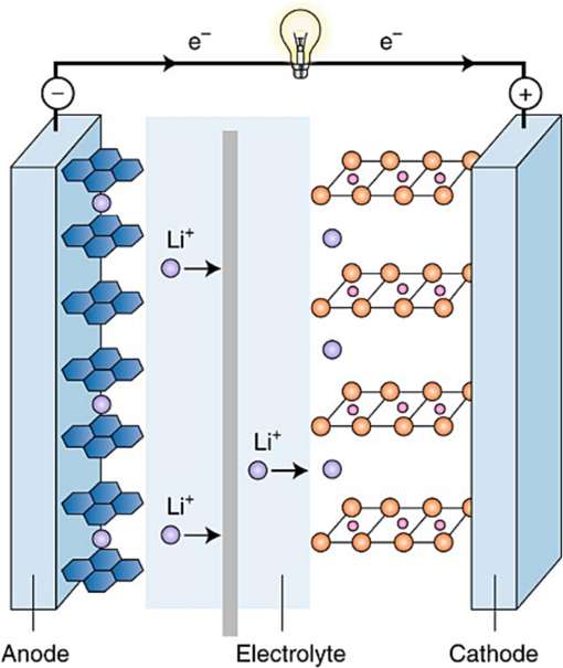
Illustrates the general sketch of fundamental operational principle of a Li-ion battery, showcasing the movement of lithium ions between the positively charged cathode and negatively charged anode through the electrolyte. Reproduced with permission from (Goodenough, 2018), Copyright 2018, Nature publishing group.
However, despite the notable energy density and extended cycle life of LIBs, they face several challenges, including the need to enhance energy and power densities, improve safety profiles, and, crucially, reduce production costs (Armand and Tarascon, 2008; Huggins, 2008; Patil et al., 2008; Xu et al., 2010; Tarascon and Armand, 2011; Choi et al., 2012; Thackeray et al., 2012; Farid et al., 2021). Currently available commercial LIBs feature graphite-based anodes and cathodes composed of lithium metal oxide or lithium iron phosphate, with theoretical capacities of 372 mAh·g−1 and less than 200 mAh·g−1, respectively (Zhang, 2011). Over the last decade, intensive research efforts have been devoted to elevating the energy and power density of LIBs. In this pursuit, silicon, with a theoretical capacity of 4200 mAh·g−1, has emerged as a highly promising candidate for anode material (Park et al., 2010; Chan et al., 2011; Wu and Cui, 2012). Notably, silicon boasts a discharge potential of 0.2 V relative to Li/Li±, a distinguishing feature when compared to other alloy-type and metal oxide anodes. Additionally, silicon ranks as the second most abundant material on Earth, (Cullis and Canham, 1991; Canham et al., 1992; Hirschman et al., 1996; Lin et al., 1997; Pavesi et al., 2000; Ding et al., 2002; Habib et al., 2018; Ali et al., 2019; Piracha et al., 2021), possesses high stability, and is non-toxic (Öğüt et al., 1997; Beard et al., 2007; Park et al., 2009; Park et al., 2010). It is characterized by remarkable carrier mobility (Park et al., 2001; Puzder et al., 2002; Warner et al., 2005) and well-established fabrication techniques (FARID et al.,; Ma et al., 2003; Jie et al., 2008; He et al., 2009; Kang et al., 2009; Peng et al., 2010; Mateen et al., 2022). These attributes collectively establish silicon as the premier material for energy storage devices.
Despite these advantages, significant challenges remain for the industrial application of silicon-based energy storage devices. Over the past few decades, various methods have been developed for fabricating micro/nano structures suitable for energy storage. These methods include reactive ion etching (Gittleman et al., 1979; Chow et al., 1987; Dussart et al., 2005; Huang et al., 2007; Chen and Hong, 2016; Huo et al., 2020), electrochemical/electroless etching (Canham, 1990; Striemer and Fauchet, 2002; Ma et al., 2006), femtoseconds laser micro structuring (Wu et al., 2001; Halbwax et al., 2008; Nayak et al., 2011; Al-Ruqeishi et al., 2017), and metal-assisted chemical etching (Peng et al., 2005a,b; Koynov et al., 2006; Peng et al., 2010; Huo et al., 2020; Huma et al., 2022). A recent study provides insights into designing high-performance anodes with large volume expansion. They used, mechanically interlocking structures inspired by biological systems, as demonstrated in the holey graphene@SiO2 anode, enhance lithium-ion storage by transmitting strain and exhibiting a mechano-electrochemical coupling effect (Wang et al., 2022). Among these fabrication techniques, metal-assisted chemical etching stands out as the most suitable, offering low cost, rapidity, minimal equipment requirements and high scalability for industrial settings.
Recent advancements in the production of Si micro/nano structures through metal-assisted chemical etching have propelled its practical application in Si-based energy storage devices. The continuous progress of this technique suggests its potential as the premier method for industrial-scale energy storage device production. This article systematically summarizes the origins and mechanisms of Metal-assisted chemical etching (MacEtch) and highlights recent achievements in the preparation of silicon micro/nano structures through this method. In recent years, the demand for high-performance materials in the development of lithium-ion batteries has grown significantly. The anode, as a crucial component, plays a pivotal role in determining the overall performance and efficiency of these batteries. This necessitates a careful consideration of the material properties required for an effective anode. Silicon nanowires have emerged as promising candidates for anode materials due to their unique features and advantages. Their high conductivity, large surface area, and compatibility with the lithium-ion battery architecture make them particularly well-suited for enhancing the performance of the anode. In this context, this paper aims to delve into the specific attributes of silicon nanowires that make them ideal for application in the anode of lithium-ion batteries.
2 Brief summary of history and mechanism of metal-assisted chemical etching (MacEtch) of silicon
In the early 1990, endeavors were initiated to explore and investigate metal-assisted etching of Silicon (Ohmi et al., 1992; Ohmi et al., 1993; Zhang et al., 1993; Morinaga et al., 1994; Morinaga et al., 1995; Jeon et al., 1996; Teerlinck et al., 1996; Gorostiza et al., 1997; Kim et al., 1997; Norga et al., 1997; Ashruf et al., 1999; Reinhardt and Kern, 2018). In 1993, Zhang et al. made the initial demonstration of luminescent porous silicon etching (Zhang et al., 1993). They utilized a polished n-type silicon surface to generate a porous silicon layer in which noble gold metal was illuminated within an HF solution containing oxygen, without the application of an external potential. Similarly, in 1997, Dimova-Malinovska et al. coated a silicon substrate with aluminum metal and then etched it using an HF-HNO3 aqueous solution to produce porous silicon (Dimova-Malinovska et al., 1997). Likewise, in 1999, Ashruf and Kelly at el. employed a p-type silicon surface to produce luminescent porous silicon in a manner akin to Zhang et al.’s approach, but without illumination (Ashruf et al., 1999). Subsequently, in 2000, Li and Bohn introduced metal nanoparticles (Au, Pt or Au/Pd) onto the surface of Si wafer that was already immersed in HF-H2O2 aqueous solution, achieving rapid preparation of light-emitting porous silicon (Li and Bohn, 2000). They uncovered that the introduction of a metal coating on the silicon surface enhanced the etching process, presenting a simple and effective way to produce porous silicon within seconds (Chattopadhyay et al., 2002; Chattopadhyay and Bohn, 2004). Although they initially named this technique “H2O2-metal-HF (HOME-HF) etching” in the main text, they ultimately termed it “metal-assisted chemical etching (MacEtch)” in the title.
In 2001, Peng et al. pioneered the preparation of silicon nanowire arrays on a silicon wafer’s surface through single-step silver-catalyzed etching in an HF-AgNO3 aqueous solution, initially referring to it as a process of self-assembling Nano electrochemistry (Peng et al., 2002; Peng and Zhu, 2003; Peng et al., 2006). They hypothesized that numerous minuscule metallic galvanic cells formed on the silicon surface during etching in the HF-AgNO3 solution. However, their initial method for silicon nanowire (SiNW) formation was later corrected in 2002 based on compelling experimental results (Peng et al., 2002; Peng et al., 2003; Peng and Zhu, 2004).
Metal-assisted chemical etching (MacEtch) is a top-down approach used for micro/nano structure fabrication (Morinaga et al., 1994; Peng et al., 2005a,b; Koynov et al., 2006; El-Bassuony and Abdelsalam, 2020; Sayed et al., 2020; Gamal et al., 2021; El-Bassuony et al., 2022a–c; Gamal et al., 2022; El-Bassuony and Abdelsalam, 2023; El-Bassuony et al., 2023; Gamal et al., 2023). Regarding the mechanism of MacEtch, extensive research has been conducted to elucidate its basic mechanism (Li and Bohn, 2000; Peng et al., 2002; Fang et al., 2006; Peng et al., 2006; Tsujino et al., 2006; Huang et al., 2007; Peng et al., 2007; Chen et al., 2008; Choi et al., 2008; Garnett and Yang, 2008; Hochbaum et al., 2008; Huang et al., 2008; Peng et al., 2008a–c; Chang et al., 2009; Geyer et al., 2009; Hildreth et al., 2009; Hochbaum et al., 2009; Huang et al., 2009; Peng et al., 2009a,b; Sivakov et al., 2009; Chen et al., 2010; Peng and Lee, 2011; Weisse et al., 2011; Hildreth et al., 2012; Li, 2012; Liu et al., 2012; Vlad et al., 2012; Liu et al., 2013; Peng et al., 2013; Chang and Sakdinawat, 2014; Chen et al., 2017). Generally, MacEtch involves a wet chemical etching process where various noble metals such as silver, gold, platinum, palladium, copper, etc., are deposited onto the surface of a silicon wafer to enhance etching at open–circuit potential (OCP) in the presence of a hydro-fluoric acid (HF) aqueous solution. Subsequently, for etching, strong oxidants like noble metal ions, nitrates, nitric acid, hydrogen peroxide, dissolved O2, etc., are employed alongside the HF aqueous solution. The etching process involves two mechanisms: electrochemical and chemical, which can be distinguished by the involvement of holes during etching at OCP. Given the presence of free holes at OCP and the influence of redox potential, this type of etching is termed electroless etching. The MacEtch of silicon at OCP in oxidizing HF aqueous solutions is essentially a noble metal catalyst-mediated electrochemical charge transfer process, wherein free holes participate, and spontaneous galvanic currents flow between local silicon anode and local metal cathode sites (Morinaga et al., 1994; Li and Bohn, 2000; Peng et al., 2002; Peng et al., 2006; Peng et al., 2008a–c; Wang et al., 2018). Hence, MacEtch of silicon is considered an electrochemical reaction. Other terms, such as metal-assisted etching, metal-catalyzed chemical etching (Li and Bohn, 2000) or metal catalyzed electrodeless etching, (Peng et al., 2005a,b) have been used in the literature instead of MacEtch (Hu et al., 2014a,b; Liu et al., 2014; Farid et al., 2019; Shafique et al., 2022; Bertran-Serra et al., 2023).
The concept proposed by Turner regarding the galvanic etching of silicon in an HF aqueous solution was validated (Turner, 1960). In this etching process, metal particles move into the bulk silicon in the same direction, facilitated by the opening of particles inducing rapid silicon dissolution. Electrically coupled metal-silicon interfaces form tiny short-circuit galvanic cells spontaneously, with the metal acting as the cathode and the silicon beneath the metal serving as the anode, leading to silicon dissolution in the HF solution, (Peng et al., 2008a–c) as depicted in Fig. 2. This process results in the movement of metal particles within the bulk silicon, accompanied by oxidation and silicon dissolution, culminating in the formation of SiNWs and Nano holes, as illustrated in Fig. 2(b, d).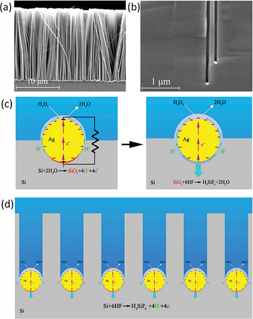
(a) Cross-sectional SEM image of aligned SiNW array prepared on p-type 7–14 Ωcm Si (1 0 0) wafer by silver-assisted etching in HF-H2O2 aqueous solution for 30 min. (b) Cross-sectional SEM view of an etched Si (1 0 0) wafer, showing straight nanoholes normal to the silicon surface and Ag particles at the bottom of the nanoholes. (c,d) Schematics of metal-assisted etching of silicon in HF-H2O2 aqueous solution. Reproduced with permission from (Peng et al., 2008a–c). Copyright 2008, Wiley-VCH.
To enhance comprehension, we will focus on the widely employed Ag-Si-HF-H2O2 MacEtch system. The following 4 equations elucidate the reactions occurring at the cathode and anode. Based on empirical findings, a process of divalent and trivalent silicon dissolution has been proposed during MacEtch in HF solution, along with the proposition of two half-cell reactions. Clearly, the overall electrochemical reactions in silicon’s MacEtch closely resemble those observed in electrochemical etching or stain etching of silicon in HF aqueous solutions containing strong oxidants. However, MacEtch distinguishes itself through the highly localized dissolution of silicon at the interface between the metal and silicon (Zhang et al., 1989; Morinaga et al., 1995; Sailor, 2012). The highly localized dissolution is pivotal because it enables precise control over the creation of nanostructures, particularly silicon nanowires (SiNWs). In MacEtch, this phenomenon contributes to the anisotropic nature of the etching process, allowing for preferential dissolution along specific crystallographic planes. This selectivity ensures the preservation of certain orientations while dissolving others, leading to well-defined nanostructures (Peng et al., 2005a,b; Peng et al., 2006). The significance lies in the ability to achieve controlled anisotropy, offering tailored nanostructures with specific characteristics. This level of precision is invaluable for applications in electronics, photonics, and sensors, where desired structural features or orientations are critical.
Cathodic reduction of oxidant at metal surface:
In the cathodic reduction step of the etching process, metal particles play a crucial role at the silicon surface. As illustrated in Fig. 2(c, d), this stage involves the reduction of oxidants facilitated by the metal surface. Metal particles, acting as catalysts, provide active sites for the reduction reaction to occur. The metal surface serves as the cathode in a galvanic cell, as shown in Fig. 2(c), with the oxidants undergoing reduction. The reduction of oxidants initiates a cascade of reactions, leading to the dissolution of silicon in the HF solution. The movement of metal particles within the bulk silicon, depicted in Fig. 2(b, d), is a result of this reduction process. This mechanism showcases the intricate interplay between metal catalysts and silicon dissolution, a fundamental aspect of the metal-assisted chemical etching process.
Anodic oxidation of silicon in contact to metal:
Overall:
In the metal-assisted chemical etching (MacEtch) process, the formation of H2SiF6 is a result of the oxidation of silicon during the movement of metal particles within the bulk silicon. H2SiF6 is a hexafluorosilicic acid, and its presence during MacEtch serves multiple purposes. Firstly, H2SiF6 acts as an etchant, contributing to the dissolution of silicon and facilitating the creation of silicon nanowires (SiNWs) and nano holes, as illustrated in Fig. 2(b, d). Secondly, the etching reaction involving H2SiF6 is crucial for the anisotropic nature of MacEtch, leading to the preferential etching along specific crystallographic planes (Peng et al., 2008a–c). The impact on SiNWs performance is two-fold. On one hand, the etching process driven by H2SiF6 contributes to the formation and refinement of SiNWs, enhancing their structural characteristics. On the other hand, careful control of the etching conditions is necessary to prevent over-etching, which could potentially impact SiNWs' performance (Peng et al., 2006). Achieving the right balance is essential to harness the benefits of H₂SiF₆ in creating well-defined nanostructures without compromising the overall performance of SiNWs.
Recently, Romano et al. (Romano et al., 2020) proposed a new method to prepare Si micro/nano structures via MacEtch of silicon in the gas phase. They demonstrate a novel method for fabricating structures with ultra-high aspect ratios in the nanoscale regime through platinum-assisted chemical etching of silicon in the gas phase. Employing a vapor of water-diluted hydrofluoric acid and continuous air flow, this technique achieves controlled etching with platinum as a catalyst, producing straight nanowires and X-ray optical elements with feature sizes as small as 10 nm. Similarly, Lukas et el, (Janavicius et al., 2023) introduces a fully programmable vapor-phase MacEtch process that generates highly uniform and unique Si nanostructures. Notable features include the versatility to produce Si micro/nano structures, various nanowire arrays with different orientations, and shapes without porosity or agglomeration. The study systematically presents different modes of precursor injection, including continuous and pulsed modes, with deterministically controlled pulse duration and period. Furthermore, the integration of a light source enables VUV-enhanced MacEtch, resulting in smoothly curved microwell structures, a feat not previously achieved. These advancements underscore the evolving landscape of MacEtch techniques, highlighting their cost-effectiveness and flexibility compared to bottom-up growth methods for Si nanostructures.
3 SiNWs prepared by metal-assisted chemical etching (MacEtch) for energy storage applications
To meet the increasing global energy requirements and the rapidly expanding market for portable electronic devices, the current focus of research is on creating economic technologies for energy storage devices. Unlike bulk silicon, silicon nanowires exhibit exceptional structural, electrical, optical, and thermal characteristics. These attributes present numerous promising avenues for applications in energy storages devices. As a result, there is a substantial global endeavor underway to advance these technologies by developing lithium-ion recharge able batteries (Chan et al., 2008; Peng et al., 2008a–c, Huang et al., 2009; Farid et al., 2024) and supercapacitors (Chang et al., 2010). In this section, SiNWs based energy storages will be reviewed.
In 2007, Chan et al. (Chan et al., 2008), employed SiNWs as anode material in Li-ion batteries. SiNWs were prepared by vapor–liquid-solid (VLS) method on stainless steel current collectors to ensure strong contact. The utilization of SiNWs offers several advantages, including their capacity to accommodate expansion, stablish strong electrical contact, and eliminate the need for binders. Notably, SiNW-based electrodes can withstand volume expansion during cycling while avoiding the pulverization that conventional Si electrodes face. SiNWs possess intrinsic strain relaxation properties, allowing for expansion in wire diameter without fissures or fractures. Moreover, to ensure robust electrical contact, SiNWs were grown on current collectors, enabling uninterrupted and efficient electron transport throughout each wire. Consequently, SiNWs collectively contribute to capacity retention as neighboring silicon nanowires maintain contact, even though expansion. This is evident in the comparison between film and particle-based silicon electrode applications, where the latter using SiNWs demonstrates an absence of material breakdown, as depicted in Fig. 3(a, b). SiNWs exhibit high discharge capacities and maintain stable cycling over tens of cycles, with reversible capacities reaching around 3400mAh/g, as illustrated in Fig. 3(c). This sustained high-capacity performance stems from the inherent ability of nanowires to endure cycling without undergoing pulverization. Unlike conventional Si particles, which suffer from continuous capacity loss due to the formation of a solid electrolyte interface (SEI) layer on new surfaces, SiNWs exhibit promise in circumventing pulverization.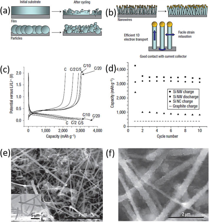
(a) Schematic of morphological changes that occur in Si during electrochemical cycling. The volume of Si anodes changes by about 400% during cycling. As a result, Si films and particles tend to pulverize during cycling. (b) SiNWs grown directly on the current collector do not pulverize or break into smaller particles after cycling. Rather, facile strain relaxation in the NWs allows them to increase in diameter without breaking. (c) The voltage profiles for the SiNWs cycled at different currents. (d) Capacity versus cycle number for the SiNWs at the C/20 rate. (e and f) SEM image of pristine SiNWs before (e) and after (f) electrochemical cycling. Reproduced with permission from (Chan et al., 2008) Copyright 2008, Nature publishing group.
The SiNWs morphology was investigated using SEM before and after electrochemical reactions to confirm their nanoscale effects and exceptional mechanical properties. Pristine SiNWs exhibited a crystalline structure with smooth sidewalls prior to lithiation, as depicted in Fig. 3(e). The average diameter of pristine SiNWs was 89 nm. After lithiation, SiNWs developed rough-textured sidewalls, with an increased average diameter of 141 nm, as shown in Fig. 3(f). Despite undergoing significant volumetric changes, SiNWs remained structurally intact and did not fragment into smaller particles. Moreover, they maintained contact with the current collector, indicating minimal capacity fading due to electrical disconnection during cycling. However, while the vapor–liquid-solid (VLS) method is effective, it poses challenges for large-scale production due to its complexity and high manufacturing costs. As a result, further research is needed to enhance fabrication method.
In 2008 Peng et al. (Peng et al., 2008a–c), firstly evaluate the characteristics of Lithium ion battery which is prepared by MacEtch SiNWs. The formation mechanism of as-prepared SiNWs anode is based on metal induced electrochemical reactions as shown in Fig. 4(a). The fabrication method has various advantages such as simplicity, large area, wafer scale and low cost. Moreover, as prepared SiNWs have good conductivity, highly rough and porous surface which allow much better accommodation of large volume changes then the VLS-CVD SiNWs, and the SiNWs have direct pathways via Si substrate allowing for efficient charge transport. Peng and co-authors show the cross-sectional view of electroless-etched SiNWs by Scanning electron microscope (SEM) in Fig. 4(b), which reveals that SiNWs are an integral part of the wafer additionally transmission electron microscopy (TEM) observation confirms the surfaces of the SiNWs are rougher than the smooth surfaces of SiNWs prepared by VLS-CVD and OAG-CVD methods. Fig. 4(c) shows the bright-field TEM image of a segment of an individual SiNW revealing clearly its rough surface. The selected-area electron diffraction pattern shows that the electroless-etched SiNW is highly single crystalline with a [1 0 0] axial orientation. Fig. 4(d) clearly displays the rough surface situated between the core and amorphous sheath of the SiNWs. This surface roughness is attributed to the lattice faceting of Si during silver-induced step-by-step HF etching. In terms of cyclic performance, the electroless-etched SiNWs demonstrate current–potential characteristics slightly different from those obtained with micro-structured Si anodes and the VLS-CVD SiNWs. The current peak is notably observed at a higher voltage, as shown in Fig. 4(e), surpassing previously reported values. Galvanostatic charge/discharge results in Fig. 4(f) reveal both the high capacity of SiNWs and voltage profiles similar to those of VLS-CVD SiNWs on stainless steel substrates. This similarity could be attributed to the formation of a solid electrolyte interface. Impressively, the cycling stability of electroless-etched SiNWs is considerably better than previous results. These SiNWs offer controllable conductivity and nanometer-scale rough surfaces, features that facilitate charge transport and the insertion/extraction of Li-ions.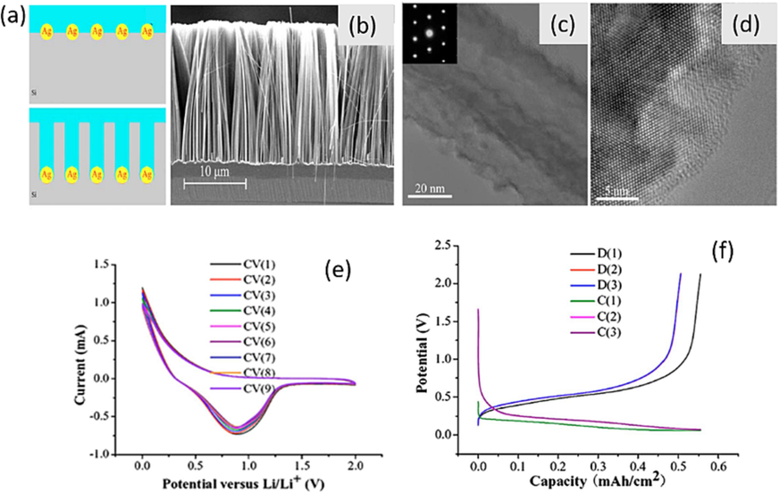
(a) Schematic formation of SiNWs via silver-induced etching. (b) Typical cross-sectional SEM image of SiNWs arrays. (c) TEM image of a segment of a single SiNW produced from Si 100 wafer. (d) HRTEM image of a SiNW, revealing the rough surface. (e) Typical cyclic voltammograms (CV) of an electroless-etched SiNWs array anode from 0 to 2 V versus Li/Li+ at a sweep rate of 1 mV s−1. (f) Voltage profiles of galvanostatic charge/discharge on an electroless-etched SiNWs array anode in the voltage range of 0.1–2.0 V versus Li/Li+ with a current density of 200 µA cm−2 (Peng et al., 2008). Copyright 2008, American Institute of Physics.
In comparison to conventionally planar-polished Si wafers, anodes made of electroless-etched SiNWs show larger capacity and longer cycling stability, revealing their potential as anode materials for high-performance rechargeable lithium-ion batteries. However, the integration of SiNWs electrodes into Li-ion batteries faces several significant hurdles, as stated in various reports. These challenges include: SiNWs prepared by MacEtch retain a bulk Si wafer beneath, limited inherent electronic/ionic conductivity, substantial volume fluctuation (∼420 %), and the progressive formation of a thick SEI film during cycling. These issues ultimately contribute to poor cycling lifespan (Liu et al., 2015; Li et al., 2017). To overcome these challenges, considerable efforts have been dedicated to coating the SiNWs with metal oxides and transferring the SiNWs from bulk Si wafers to other substrates.
To overcome the aforementioned challenges, Mingyuan et al. (Ge et al., 2012) pioneered the fabrication of porous doped silicon nanowires by Metal-assisted chemical etching (MacEtch) method for Li-ion batteries in 2012. They demonstrated the direct etching of boron-doped silicon wafers to produce these porous silicon nanowires. In addition, they used commercially available alginic acid sodium salt as a binder, which exhibits a viscosity of 2000 cP at 2 wt%. These nanowires demonstrated exceptional electrochemical performance and extended cycle life when employed as anode material in lithium-ion batteries, with alginate serving as the binder. Even after 250 cycles, the capacity remains stable above 2000, 1600, and 1100 mAh/g at current rates of 2, 4 and 8 A/g, respectively. This demonstrates the high structural stability due to the high porosity and electron conductivity of the porous silicon nanowires. Despite this success, alginic acid sodium salt has not yet been fully explored for battery studies.
Moreover, G. Sandu et al. (Sandu et al., 2018) demonstrated a novel electrode configuration for Li-ion batteries, employing three-dimensional interweaving kinked silicon nanowires (k-SiNWs) integrated with a Ni current collector. The scalable production of k-SiNWs was achieved through a continuous metal-assisted chemical etching process of silicon, complemented by a chemical peeling step enabling the silicon substrate’s reuse. The kinks in the nanowires were generated through a simple and repetitive etch-quench cycle in an etchant composed of HF and H2O2 as shown in Fig. 5.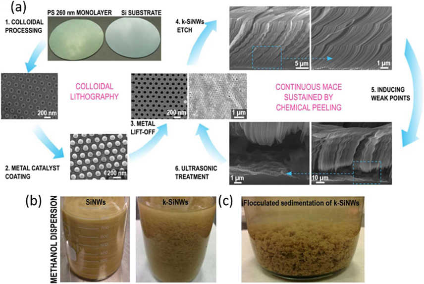
Kinked SiNWs synthesis and processing. Continuous synthesis of k-SiNWs sustained by chemical peeling (a). The first step is the nanopatterning of the metal catalyst mask, conveniently achieved by colloidal lithography with polystyrene spheres. Their diameter can be customized by reactive ion etching (1). The holey Au mask can be obtained after the coating of the patterned Si substrate with a thin film (2) and the subsequent removal of the polystyrene spheres (3). The main fabrication step involves etching in a solution containing HF and H2O2. The etching parameters are favorable for non–〈1 0 0〉 etching directions. Interrupting the etching at certain points induces changes in the etching direction and triggers the formation of kinks between adjacent segments (4). When the desired length is achieved, the etching conditions are again modified to favor the presence of a porous segment at the base of the k-SiNW’s (5). This porous segment facilitates the separation of k-SiNWs from their Si substrate with a short ultrasonic treatment, leaving the metallic mask intact and ready for a new etching sequence (6). Dispersion of SiNWs vs. k-SiNWs in methanol (b). Optical image of the flocculated sedimentation of k-SiNWs (c).(Sandu et al., 2018) Copyright 2018, Nature publishing group.
The high anisotropic nature of the Metal-assisted Chemical Etching (MacEtch) process, which distinguishes it significantly from conventional wet-etch methods, can be attributed to the preferential etching along specific crystallographic axes of the silicon substrate (Peng and Zhu, 2004; Peng et al., 2005a,b; Peng et al., 2006; Peng et al., 2007; Peng et al., 2008a–c). In MacEtch, the anisotropy arises from the complex interplay between the metal catalyst, typically noble metals like gold or silver, and the silicon substrate. The metal catalyzes the etching reaction, leading to the formation of metal-silicon complexes. The selectivity of MacEtch for specific crystallographic planes, such as the (1 0 0) plane, is influenced by the surface energy and reactivity of these planes (Peng et al., 2005a,b; Peng et al., 2008a–c). The high anisotropy in MacEtch is a result of the differential reactivity of the crystallographic planes. The metal catalyst preferentially binds to certain planes, promoting faster etching along those planes compared to others. This preference is due to the orientation-dependent surface energy and chemical reactivity of the silicon crystal lattice. Conversely, conventional wet-etch methods typically lack the specificity seen in MacEtch. In conventional wet etching, the etchant reacts uniformly with the entire exposed surface, leading to isotropic etching without a pronounced preference for specific crystallographic orientations. In summary, MacEtch achieves high anisotropy through the selective interaction between the metal catalyst and specific crystallographic planes of the silicon substrate. This unique characteristic makes MacEtch a powerful and precise technique for creating well-defined nanostructures, such as the kink-nanowires shown in Fig. 5.
Their findings indicate that the interconnected structure formed by k-SiNWs and multi-walled carbon nanotubes possesses advantageous mechanical properties, displaying a foam-like behavior that enhances deformation during Li-insertion. Furthermore, the integration of ionic liquid electrolyte systems with the Ni current collector helps mitigate the adverse effects associated with Si-Li alloying reaction, leading to remarkable cycling stability with 80 % capacity retention (1695mAh/gSi) following 100 cycles. Notably, an areal capacity of 2.42 mAh/cm2 can be achieved at the maximum assessed thickness corresponding to 1.3 mg Si/cm2.
In 2023 A.D Refino et al. (Refino et al., 2023) synthesized a dense monocrystalline vertical SiNWs using metal-assisted chemical etching (MacEtch) directly from a silicon wafer. Subsequently, Li metal deposition was performed through thermal evaporation. Initial reactions between Li and Si were observed in planar Si anodes, resulting in the production of a lithiated LixSiy phase situated between bulk Si and the thin film of Li metal. However, the pre-lithiation process with higher Li concentration exclusively occurred on the upper region of vertically aligned SiNWs. This indicates that during the deposition of Li metal, the sidewalls of the dense SiNWs were not fully covered. Notably, their electrochemical cycling investigations have illuminated the significant influence of Li metal exposure on the electrochemical performance of Si anodes. In the case of planar Si, the presence of Li metal exposure led to the generation of more electrochemically active sites that facilitate Li-Si phase formation reaction during the de-lithiation process. Furthermore, the accumulated Li metal acted as a reservoir to counteract severe active lithium loss. In SiNWs, the incomplete coverage of the SiNWs forest surfaces with Li metal during deposition resulted in a distinct lithiation behavior compared to planar Si. This non-uniform alloying prompted the formation of non-uniform electroactive regions, underscoring its contributions to this distinct behavior. A subsequent post-mortem analysis unveiled a layer-like structure at the top of the pre-lithiated SiNWs, a feature absents in pristine SiNWs. Moving forward, future investigations should be directed towards developing a technique for the conformal coating of the SiNWs with Li. Such a method would offer deeper insights into the essence of three dimensional pre-lithiation and its implications on the performance of Li-ion batteries.
A.Vlad et al. (Vlad et al., 2012) present a novel method for the fabrication of roll-out Li-ion battery components derived from silicon chips. Their process involves a continuous and repeatable cycle of etching, infiltrating and peeling. Initially, vertically aligned SiNWs are etched by metal-assisted chemical etching method, from recycled silicon wafers, as shown in Fig. 6(a). These SiNWs are then embedded in a polymer matrix that serves as both a Li-ion gel electrolyte and an electrode separator as shown in Fig. 6(b). Subsequently, the entire structure is peeled off, allowing for the fabrication of multiple battery devices from the single silicon wafer. Even after undergoing multiple fabrication steps, including silicon MacEtch, polymer infusion, and lithium-polymer silicon nanowire (LIPOSIL) composite peeling, the mask remains intact and continues to produce high-quality nanowires arrays as show in the Fig. 6(c-e). The primary constraint in the current fabrication process is the initial thickness of the Si chip. For instance, the MacEtch mask can still be utilized after delaminating four composite membranes (Fig. 6c) from 330 µm thick Si chip. They attain an initial discharge capacity of ∼ 3500 mAh/g at C/20 cycling rate, where C-rate is defined as 1C equivalent to a 1-hour discharge.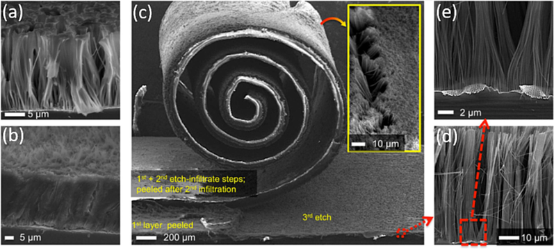
Polymer infiltration and multi-peeling protocol. (a) Partial infiltration showing the conformal coating of single and bunches of nanowires. (b) Fully infiltrated Si nanowires. (c) Exemplification of the multi-loop etch-infiltrate-peel protocol. Three consecutive etch-infiltrate-peeling processing loops have been performed on the same Si chip and using the same MACE mask. (Inset) Back-side of the peeled membranes, showing the exposed nanowires for current collector contact. (d,e) Even after several etch-infiltrate-peel steps, the MACE mask maintains its integrity and continues to provide high-quality Si nanowires arrays, (Vlad et al., 2012) Copyright 2012, proceedings of the national academy of sciences of the United states of America.
The capacity loss in the first cycle is ∼ 1000 mAh/g, which is attributed to the structural imperfections, unintended disruption of electrical contact between the high aspect ratio SiNWs and the thin film current collector, and the formation of the SEI film. It’s worth noting that the electrochemical performance is significantly impacted by the mechanical peeling process. The process entails using a laboratory stainless-steel blade, which is manually manipulated to crack the base of the nanowires and remove the LIPOSIL composite. This procedure results in partial damage to the SiNWs, particularly at the peeled base, as indicated by the presence of dusty residuals on the blade, substrate and LIPOSIL membrane.
To enhance electrical conductivity and protect the surface of the SiNWs against direct exposure to the electrolyte, a thin Cu layer has been introduced on the SiNWs’ surface, as shown in Fig. 7(a), via physical vapor deposition. This metal layer exhibits uniformity and conforms to the entire length of the SiNW (Fig. 7(b)). By precisely controlling the growth time, it can be tailored into a porous structure consisting of interconnected Cu grains that decorate the SiNW surface. This structure results from the electroless reduction of Cu2+ ions at the surface. During the initial stages of deposition, the SiNWs are adorned with a discontinuous layer of Cu nanoparticles, which then evolve into a continuous porous network as the deposition process continues. Extended deposition ultimately leads a thick and continuous Cu matrix that encapsulates the SiNWs. The porous and interconnected configuration of the Cu shell can be envisioned as a metallic grid enwrapping the nanowires and electrically connected to the current collector, as show in Fig. 7(c). This arrangement is anticipated to enhance the electrochemical stability and cycling rate performance of the LIPOSIL composite. The metallic properties of the Cu shell enhance the electrical conductivity of the SiNWs, thereby improving charge collection efficiency (Chen et al., 2011; Zhang et al., 2011; Zhang and Braun, 2012; Farid et al., 2023). Simultaneously, the porous structure of the shell facilitates rapid diffusion of Li+ ions towards the surface of the SiNWs. This porosity also aids in preserving the structural integrity of the SiNWs, thanks to the ductile nature of copper. Comparing this design to the reverse configuration, where Cu forms the core and Si the shell (Cu-core@ Si-Shell), the Si-core@ Cu-Shell design is expected to offer similar performance with regard to charge collection efficiency. As anticipated, the LIPOSIL composite featuring Si-core@ Cu-Shell nanowires shows improved performance compared to the LIPOSIL composite with pristine SiNWs, as shown in Fig. 7(d). The first discharge capacity of 3900 mAh/g is higher than for pristine SiNWs, and the composite with Cu-Shell nanowires is able to sustain a capacity of ∼ 2000 mAh/g over extended cycling with little capacity fading. This equates to ∼ 4 mAh/cm2 or ∼ 1600 mAh/cm3, placing it in competition with commercial anode formulations with capacities falling within the range of approximately 3–5 mAh/cm2 (Liang et al., 2019). While the initial capacity loss in the first cycle is likely attributed to the structural imperfection and contact issues with the thin film current collector, the composite with pristine SiNWs exhibits more noticeable degradation during cycling. The notable improvement is clearly attributed to the enhanced conductivity conferred by the Cu-coated SiNWs. Fig. 7(e), provides a detailed view of the high-rate cycling results for the Si-core@ Cu-Shell LIPOSIL and the bare LIPOSIL composite films. A stable nominal capacity is achieved at a C-rate of C/20. Subsequent cycling is carried out at higher current rates, as depicted in Fig. 7(f). Remarkably, the Si-core@ Cu-Shell nanowires in the LIPOSIL composite outperform the uncoated nanowires by delivering significantly higher capacity as the cycling rate increases. For instance, at a 1C rate, the Si-core@ Cu-Shell-LIPOSIL composite exhibits a reversible capacity of ∼ 1000mAh/g, whereas the uncoated nanowires provide around 350 mAh/g. Furthermore, the Si-core@ Cu-Shell composite, as LIPOSIL, maintains its rated capacity even during operation at reduced current rates.(Iftikhar et al., 2023) High-rate electrochemical investigations demonstrate that the Si-core@ Cu-Shell-LIPOSIL electrode–electrolyte composite exhibits potential as a valuable material for high-rate electrode application. This study offers a resolution for the management of electronic waste by offering a secondary utilization for the silicon through the utilization of LIPOSIL anodes recovered from discharged silicon chips at the end of their lifecycle. As shown, this idea has proven practical in a laboratory setting and has the potential to be economically feasible when implemented on a large scale.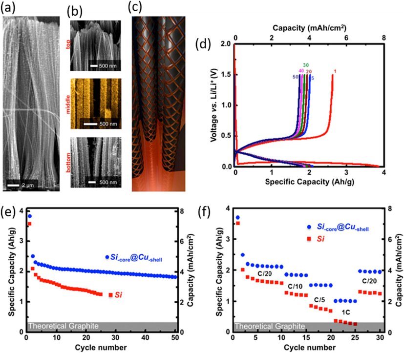
Improving the electrochemical performance of composite anodes through conformal copper coating. (a) Conformal Cu coating of high aspect ratio Si nanowires with coaxial morphology through an electroless deposition protocol. (b) Snapshots at different height positions evidencing the uniform Cu coating along the Si nanowires. (c) Schematic representation of the Cu-wrapped Si nanowires. The Cu shell has a porous, electrically interconnected structure to allow for a faster Li+ insertion, volume expansion accommodation and efficient current collection. (d) Discharge/ charge profiles for the Si-core @ Cu-shell composite anodes cycled between 1.5 and 0.02 V. (e) Capacity retention at a cycling rate of C/20 of the Si and Si-core @ Cu-shell polymer electrolyte composite anodes. (f) Rate capability of the Si and Si-core @ Cu-shell polymer electrolyte composite anodes. The theoretical capacity of graphite is highlighted for comparison, (Vlad et al., 2012) Copyright 2012, proceedings of the national academy of sciences of the United states of America.
It is desirable to transfer of SiNWs arrays from bulk Si wafer substrate to alternative substrates, particularly flexible ones for use in flexible devices. Weisse and Zheng et al. (Weisse et al., 2011), have introduced an exciting and simple method for this purpose. They achieved the vertical transfer of SiNWs arrays with consistent lengths onto diverse substrates by inducing horizontal crack on SiNWs. This crack formation process involves immersing an Ag-MacEtch SiNWs sample in water and subsequently subjecting it to Ag-assisted etching processes. The authors proposed that the formation of these cracks is linked to the delamination and reattachment of an Ag film during the soaking process in water. However, it’s worth noting that this simple water-soaking crack method is ineffective for the delaminating and reattaching the gold film. Also, it is a very time-consuming and lengthy process. Furthermore, the explanation was not clear regarding how Ag delaminated and reattached. The cracked method simplifies the process of embedding SiNWs within polymers and integrating them into channels. This, in turn, enables the creation of SiNWs that possess both mechanical flexibility and scalability to larger dimensions.
G. Farid et al. (Farid et al., 2022) presented for the first time, an explanation that the oxidative dissolution of silver in hot water, facilitated by dissolved oxygen, crucially initiates crack formation in Ag-MacEtch SiNWs arrays. They have developed a comprehensive approach to rapidly induce horizontal cracks in membranes of MacEtch SiNWs arrays using metal etchants. This method enables swift metal dissolution, followed by spontaneous metal reformation, allowing for the fabrication of MacEtch SiNWs. In case of Ag-assisted etched SiNWs soaked in hot deionized (DI) water, the dissolved oxygen in the water gradually dissolves Ag, transforming it into Ag-ions. These Ag-ions do not persist in this state; instead, they spontaneously reform on the root sidewall of SiNWs as Ag particles. The newly formed Ag-particles on the root side walls of SiNWs act as catalysts for silicon etching along the horizontal direction, resulting in the cutting of SiNWs. Simultaneously, the undissolved Ag particles located at the base of SiNWs continue to catalyze Si etching, causing the elongation of SiNWs. This complex process ultimately leads to the formation of cracks that run parallel to the wafer surface across large area aligned SiNWs. It is important to note that the dissolution rate of Ag in hot DI water (H2O) is relatively slow due to the limited presence of dissolved oxygen and the sluggish kinetics of the oxygen reduction reaction. Consequently, crack formation in Ag-etched SiNWs using hot water requires a long soaking time. The oxygen dissolved in water serves as a relatively mild green oxidant, while hydrogen peroxide (H2O2) represents a potent and environmentally friendly oxidant alternative. Indeed, H2O2 proves to be considerably more potent oxidant compared to dissolved molecular oxygen. It exhibits rapid reactivity with Ag, leading to the swift release of Ag-ions within a matter of seconds.
The rate of oxidative dissolution of Ag by H2O2-H2O at room temperature is approximately 100 times faster than that observed with hot DI water during the initial stage of soaking. Inspired by the remarkable ability of H2O2-containing DI water to dissolve Ag effectively at room temperature, incorporating H2O2-containing DI water soaking into the process between Ag-assisted etched steps will facilitate rapid crack formation throughout SiNWs arrays. This approach offers the advantage of avoiding the need for time-consuming and high-temperature soaking, as shown in Fig. 8(a). Fig. 8(b) shows a typical SEM image of a vertically aligned SiNW arrays on a p-Si (1 0 0) wafer. This array was obtained through Ag-assisted etched in an aqueous HF- H2O2 solution for 30 min. Following a 1-minute soaking in H2O2-contained DI water at room temperature and subsequent etching in an aqueous HF- H2O2 solution for another 30 min, a uniform horizontal crack emerged between the original upper SiNW array and the newly formed lower SiNW arrays, as shown in Fig. 8(c). This demonstrate that the use of H2O2-contained DI water reduces the soaking time from 3 h to just 1 min or less, effectively initiating the formation of cracks in Ag-assisted etched SiNWs.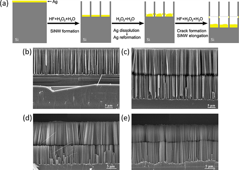
(a) Schematic illustration of rapidly generating horizontal crack in silver-assisted etched SiNWs by introducing silver etching in aqueous H2O2 solution between two consecutive silver-assisted etching of silicon in HF−H2O2 aqueous solutions. (b) Typical SEM image of SiNW array on 1–10 Ω·cm p-Si (1 0 0) wafer produced by silver-assisted etching of silicon in HF−H2O2 aqueous solution. (c), (d) and (e), typical SEM images of cracked SiNW array on 1–10 Ω·cm p-Si (1 0 0) wafer, 0.005 Ω·cm p-Si (1 0 0) wafer and 0.008 Ω·cm n-Si (1 0 0) wafer, respectively, generated by soaking silver-assisted etched SiNW array in H2O2 aqueous solution for 1 min and then etching in HF−H2O2 aqueous solution. All the experiments were performed at room temperature (25 °C). (Farid et al., 2022) Copyright 2022, American Chemical Society.
It’s worth noting that this uniform crack formation can be achieved in Ag-assisted Etched SiNWs formation on Si wafer with varying doping types and concentrations, as shown in Fig. 8(d, e). These uniform horizontal cracks significantly weaken the connection between the upper and lower SiNW array layers by partially etching the silicon that bridges them at the location of the crack. Unlike silver, gold (Au) is highly stable and shows minimal oxidative dissolution when exposed to both natural and H2O2-containing DI water during soaking. This inherent stability of gold is the reason why cracks cannot form in Au-assisted etched SiNW when subjected to hot DI water or H2O2-containing DI water. Wet etching of Au plays a crucial role in microfabrication processes, and over the past few decades, numerous Au etchants have been developed. Aqueous Au etchants typically consists of two key components: a potent oxidizing agent and a complexing ligand.
One of the most practical alternatives to aqua regia for Au etching is the utilization of H2O2 in combination with an aqueous hydrochloric acid (HCL) solution, known as HCL/H2O2/H2O. This particular solution is widely employed in the wet cleaning of silicon surfaces, where it effectively removes various trace metals. The oxidative dissolution behavior of gold in HCL/H2O2/H2O is analogous to that of Ag in H2O2/H2O. In this process, the dissolved gold ions do not persist in their ionic form; instead, they reassemble as metallic gold on the silicon surface in the form of particles. This transformation occurs as the gold ions extract electrons from the silicon. The oxidative dissolution of Au by H2O2 in the presence of HCl-containing DI water, followed by the reformation of Au particles, suggests that HCL/H2O2/H2O soaking between successive Au-catalyzed etching steps of silicon leads to the desired rapid formation of cracks in Au-assisted etched SiNW. Consequently, this process facilitates the uniform transfer of the upper SiNW array layer onto a foreign substrate, as show in Fig. 9.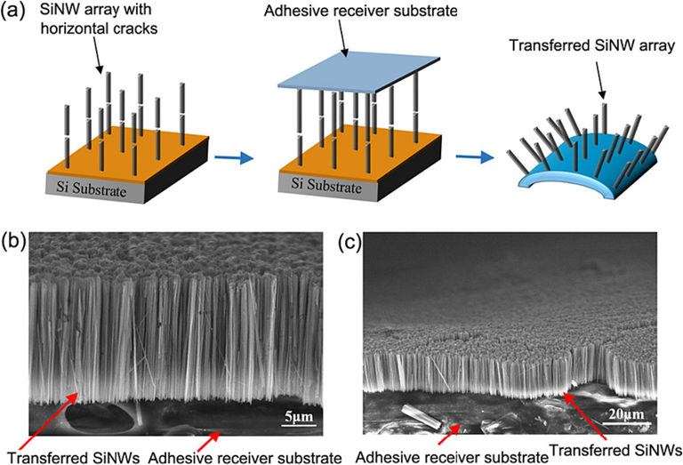
(a) Schematic illustration of adhesive substrate-assisted peeling off cracked metal-assisted etched SiNW array from its bulk silicon matrix. (b) and (c), SEM images of the vertical SiNW array transferred to an adhesive tape.(Farid et al., 2022) Copyright 2022, American Chemical Society.
The fast metal dissolution achieved through wet metal etchants significantly shortens the soaking process, reducing it from 3 h to just 1 min or even less at room temperature. This research provides valuable insights for fabricating cracked SiNWs arrays, focusing on simplicity and scalability. This paves the way for the mass production of SiNWs-based fexible devices such as batteries, making them more accessible and practical for various applications.
H. Kim et al. (Kim et al., 2013) introduced an innovative vertical transfer technique for SiNWs grown on a silicon substrate, allowing direct attachment to current-collecting electrode without the need for a polymer adhesive. This advancement is specifically tailored for use as a binder-free anode in lithium-ion batteries. The vertical aligned SiNWs, fabricated through a cost-effective, large-scale metal-assisted chemical etching process, have been effectively transposed onto a copper electrode coated with a thin layer of Silver (Ag) using a straightforward hot-pressing method (Shen et al., 2023). The SiNWs arrays, oriented vertically, of exhibit consistent lengths following the initial MacEtch process. These SiNWs arrays are subsequently separated into two layers with uniform lengths of ∼ 60 µm, after the first etching and 1.5 µm after the second etching, facilitated by the formation of horizontal cracks, as shown in Fig. 10(a). (Weisse et al., 2012).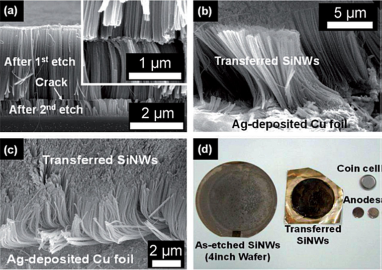
(a) Cross-sectional FE-SEM image of the as-prepared SiNW arrays with horizontal crack on Si substrate. Inset: Zoom-in image of the horizontal crack. (b) Cross-sectional FE-SEM image of the central surface of 10 mm long SiNWs transferred onto the Ag-coated Cu electrode. (c) Tilted-surface FE-SEM image of the outer edges of the transferred 10 mm long SiNWs. (d) Photographs of as-prepared SiNWs on Si substrate, vertically transferred SiNWs on Cu electrode, as-prepared SiNW anodes, and coin-type half-cell (Kim et al., 2013). Copyright 2013 Wiley-VCH Verlag GmbH & Co. KGaA, Weinheim.
A closer examination, as depicted in the inset of Fig. 10(a), reveals partial etching of the silicon material at the crack locations, resulting in a weakened connection between the upper and lower SiNW array layers. To facilitate the transfer of the SiNW arrays from the crack location, a thin silver (Ag) buffer film was utilized as an adhesion layer due to its ability to promote solid-state bonding (Wang and Lee, 2009; Kroupa et al., 2012) and its fluidic mobility at elevated temperatures (Oh and Jeong, 2012). Fig. 10(b, c) show the SiNWs after their transfer onto copper foil coated with an Ag layer, clearly illustrating a vertically oriented SiNW layer.
Notably, the upper segments of the transferred SiNWs do not aggregate into bundles, differing from the behavior of the as-etched SiNWs. This observation suggests that the original as-etched SiNWs on the Si wafer primarily cluster at their uppermost sections. Consequently, the lower part of the originally as-etched SiNWs becomes the upper section of the transferred SiNWs. The central regions of the transferred SiNWs exhibit an upright orientation, as shown in Fig. 10(b), whereas SiNWs at the outer edges exhibit bending at their bases (Fig. 10(c)). Furthermore, the transfer process reveals that the SiNWs are partially embedded within the Ag thin film layer.
In Fig. 10(d), a series of photographs illustrate different stages of the process, including as-etched SiNWs, vertically transferred SiNWs on a copper electrode coated with Ag, SiNWs anodes prepared, and coin-type half-cell. The SiNWs arrays produced by MacEtch process can be seamlessly transferred in a vertical orientation onto the copper electrode, achieved by utilizing a thin layer of Ag without the need for polymer adhesives. This achievement was made possible through the dry transfer-printing method, a crucial step in realizing Li-ion batteries.
Upon assessment as a Li-ion battery anode, without the reliance on traditional polymeric binders or conducting additives, the vertically aligned SiNWs that had been successfully transferred displayed remarkable performance attributes. Specifically, they exhibited a substantial specific capacity of ∼2150 mAh/g and exceptional rate performance. This success can be attributed to the simplicity and efficiency of the anode manufacturing process. This streamlined approach not only enables cost-effective, large-scale production but also holds broad applicability, paving the way for innovative advancements in the rational design of silicon-based electrode materials, enhancing power density and conductivity.
In the realm of advanced energy conversion and storage, the allure of silicon nanostructures is undeniable, presenting a pathway to a sustainable future with their exceptional structural, electrical, optical, and electrochemical properties. Amidst the various top-down approaches, Metal-assisted Chemical Etching emerges as a transformative method, distinguished by its cost-effectiveness, simplicity, versatility, and scalability. Recent breakthroughs have elevated MacEtch to a position of prominence, establishing it as the preferred technique for crafting micro/nano structures endowed with remarkable electrochemical attributes. These structures, meticulously tailored through MacEtch, are poised to revolutionize energy storage applications, spanning from LIBs to supercapacitors. We unravel the intricacies of MacEtch's silicon transformation and delve into the latest advancements in SiNWs, particularly their electrochemical prowess for energy storage applications.
4 Future prospects for SiNW electrodes
The future prospects for SiNW electrodes are promising, particularly within the realm of Li-ion batteries, for several compelling reasons:
-
Rapid lithiation and delithiation: SiNWs electrodes exhibit a remarkable ability to undergo rapid lithiation and delithiation processes with reduce kinetic barriers, contributing to faster charging and discharging rates in Li-ion batteries.
-
Volume expansion management: SiNWs possess the unique capability to accommodate the volume expansion that occurs during the lithiation process. This expansion is effectively managed with the lateral porous spaces between the nanowires, ensuring structural integrity over repeated charge–discharge cycles.
-
Versatile synthesis method: The wide range of SiNW synthesis methods available offers hope for the development of commercially viable SiNW electrodes. These methods allow for tailoring the properties of SiNWs to meet specific Li-storage capacity and cycling stability requirements.
-
Integration into existing processes: SiNWs fabricated using MacEtch process can be seamlessly integrated into existing electrode fabrication processes. The SiNWs prepared by etching Si wafer substrates can be directly cut from the etched wafer without the need for conductive additives and binders. This approach allows for straightforward integration, including in electronic components such as on-chip batteries.
To fully realize the potential of SiNWs electrodes, future efforts should prioritize the following areas of optimization:
-
Streamlining fabrication processes: Streamlining the fabrication processes for SiNWs can help reduce complexity and cost, making them more accessible for large-scale production.
-
Improving the long-term cycling stability: Improving the long-term cycling stability of SiNW electrodes is critical for their practical use in Li-ion batteries. Strategies to mitigate capacity fading over numerous charge–discharge cycles are essential.
-
Reducing manufacturing costs: Lowering the overall manufacturing cost of SiNW electrodes will be pivotal in their widespread adoption and commercial viability.
As our understanding of the lithiation and delithiation behaviors of SiNWs continues to improve, it is highly likely that high-capacity SiNW electrodes will play a significant role in advancing the development of next-generation Li-ion batteries. Their unique properties make them a promising candidate for improving energy storage technology.
5 Concluding remarks and future perspectives
In summary, this comprehensive review thoroughly examines the origin, mechanism, and progression of the MacEtch process applied to silicon in an oxidizing hydrofluoric acid (HF) solution. A particular focus is given to its application in fabricating Li-ion batteries using SiNWs. Despite MacEtch's extensive research history, it remains a subject of ongoing debate within the scientific community. The electrochemical galvanic etching process involves anodic and cathodic reactions at the silicon surface, mediated by noble metals. However, this broad electrochemical framework lacks a comprehensive understanding of the specific mechanisms driving the etching process, necessitating further in-depth investigations. SiNWs, produced through the MacEtch process, show significant potential for emerging energy storage applications, especially in Li-ion batteries. These SiNWs offer advantages such as exceptional lithium storage capacity, stress accommodation for reversible lithiation/delithiation, and rapid charge/discharge rates. This promise is enhanced by the ability to finely control morphological features and electrical properties. Moreover, the simplicity of the MacEtch process makes it suitable for scalable production in various energy-related applications.
However, the Vapor-Liquid-Solid growth method for SiNWs, despite its progress in the context of LIBs, may face cost-related challenges due to its high-temperature process. Additionally, SiNWs' ultrahigh surface area can lead to substantial solid electrolyte interface formation, necessitating controlled management. To fully unlock the potential of SiNW anodes, simultaneous advancements in LIBs cathode technology are crucial. A holistic approach addressing challenges in both anode and cathode materials will be pivotal in advancing Li-ion battery technology. The ongoing exploration and understanding of the MacEtch process, coupled with advancements in SiNW synthesis and integration techniques, hold the promise of yielding even more efficient and high-performing energy storage solutions in the future. The journey toward superior energy storage continues, guided by a deeper understanding of nanoscale materials and their intricate electrochemical behaviors.
CRediT authorship contribution statement
Ghulam Farid: Conceptualization, Validation, Formal analysis, Writing – original draft. Roger Amade-Rovira: Writing – review & editing, Funding acquisition, Supervision. Yang Ma: Writing – review & editing, Formal analysis, Validation. Stefanos Chaitoglou: Writing – review & editing, Formal analysis, Validation. Rogelio Ospina: Writing – review & editing, Formal analysis, Validation. Enric Bertran-Serra: Writing – review & editing, Funding acquisition, Supervision.
Acknowledgments
The publication of this article is funded by Grant PID2020-116612RB-C32 funded by MCIN/AEI/ 10.13039/501100011033 and by the “European Union” or by the “European Union Next Generation EU/PRTR. The authors acknowledge financial support from projects PID2020-116612RB-C32, PDC2021-121868-C22, TED2021-132070B-C21, TED2021-131442B-C33 funded by MCIN/AEI/10.13039/501100011033 and, as appropriate, by “ERDF A way of making Europe”, by the “European Union” or by the “European Union Next Generation EU/PRTR”. The ENPHOCAMAT group acknowledges support from the AGAUR of Generalitat de Catalunya, Project No. 2021SGR00936. One author (G.F.) acknowledges the support from the predoctoral fellowship PREDOCS-UB (APIF) funded by the MICINN of Spanish Government. Another author (S.C.) acknowledges support from the postdoctoral fellowhips programme Beatriu de Pinós, funded by the Secretary of Universities and Research (Government of Catalonia) and by the Horizon 2020 programme of research and innovation of the European Union under the Marie Sklodowska-Curie grant agreement No 801370 (H2020-MSCA-COFUND-2017). One author (R.O.) acknowledges the financial support from the Requalification of the Spanish University System 2021-23 program funded by the Next Generation EU program through the Ministry of Universities of Spanish Government. Another author (Y.M.) acknowledges the support from the predoctoral fellowship funded by the Chinese Scientific Fellowship program of the Chinese Government.
References
- Biomimetic brain-like nanostructures for solid polymer electrolytes with fast ion transport. Sci. China Mater.. 2022;65:1476-1484.
- [Google Scholar]
- Facile microemulsion synthesis of vanadium-doped ZnO nanoparticles to analyze the compositional, optical, and electronic properties. Materials. 2019;12:821.
- [Google Scholar]
- Direct growth and photoluminescence of silicon nanowires without catalyst. Arab. J. Chem.. 2017;10:S2025-S2031.
- [Google Scholar]
- Galvanic porous silicon formation without external contacts. Sens. Actuat., A. 1999;74:118-122.
- [Google Scholar]
- Multiple exciton generation in colloidal silicon nanocrystals. Nano Lett.. 2007;7:2506-2512.
- [Google Scholar]
- Advancements in plasma-enhanced chemical vapor deposition for producing vertical graphene nanowalls. Nanomaterials. 2023;13:2533.
- [Google Scholar]
- Climate sensitivity uncertainty and the need for energy without CO2 emission. Science. 2003;299:2052-2054.
- [Google Scholar]
- Silicon quantum wire array fabrication by electrochemical and chemical dissolution of wafers. Appl. Phys. Lett.. 1990;57:1046-1048.
- [Google Scholar]
- Efficient visible electroluminescence from highly porous silicon under cathodic bias. Appl. Phys. Lett.. 1992;61:2563-2565.
- [Google Scholar]
- High-performance lithium battery anodes using silicon nanowires. Nat. Nanotechnol.. 2008;3:31-35.
- [Google Scholar]
- High-performance lithium battery anodes using silicon nanowires. In: Materials for Sustainable Energy: A Collection of Peer-Reviewed Research and Review Articles from Nature Publishing Group, World Scientific. 2011. p. :187-191.
- [Google Scholar]
- Densely packed arrays of ultra-high-aspect-ratio silicon nanowires fabricated using block-copolymer lithography and metal-assisted etching. Adv. Funct. Mater.. 2009;19:2495-2500.
- [Google Scholar]
- Fabrication of silicon nanopillar-based nanocapacitor arrays. Appl. Phys. Lett.. 2010;96
- [Google Scholar]
- Ultra-high aspect ratio high-resolution nanofabrication for hard X-ray diffractive optics. Nat. Commun.. 2014;5:4243.
- [Google Scholar]
- Direct-write patterning of microstructured porous silicon arrays by focused-ion-beam Pt deposition and metal-assisted electroless etching. J. Appl. Phys.. 2004;96:6888-6894.
- [Google Scholar]
- In-plane control of morphology and tunable photoluminescence in porous silicon produced by metal-assisted electroless chemical etching. J. Appl. Phys.. 2002;91:6134-6140.
- [Google Scholar]
- 0.76% absolute efficiency increase for screen-printed multicrystalline silicon solar cells with nanostructures by reactive ion etching. Sol. Energy Mater. Sol. Cells. 2016;157:48-54.
- [Google Scholar]
- Controlling kink geometry in nanowires fabricated by alternating metal-assisted chemical etching. Nano Lett.. 2017;17:1014-1019.
- [Google Scholar]
- Wafer-scale synthesis of single-crystal zigzag silicon nanowire arrays with controlled turning angles. Nano Lett.. 2010;10:864-868.
- [Google Scholar]
- Morphological Control of Single-Crystalline Silicon Nanowire Arrays near Room Temperature. Adv. Mater.. 2008;20:3811-3815.
- [Google Scholar]
- Silicon nanowires coated with copper layer as anode materials for lithium-ion batteries. J. Power Sources. 2011;196:6657-6662.
- [Google Scholar]
- Challenges facing lithium batteries and electrical double-layer capacitors. Angew. Chem. Int. Ed.. 2012;51:9994-10024.
- [Google Scholar]
- Synthesis of silicon nanowires and nanofin arrays using interference lithography and catalytic etching. Nano Lett.. 2008;8:3799-3802.
- [Google Scholar]
- Reactive ion etching of silicon in CCl4 and HCl plasmas. J. Electrochem. Soc.. 1987;134:1281-1286.
- [Google Scholar]
- Visible light emission due to quantum size effects in highly porous crystalline silicon. Nature. 1991;353:335.
- [Google Scholar]
- Preparation of thin porous silicon layers by stain etching. Thin Solid Films. 1997;297:9-12.
- [Google Scholar]
- Electrochemistry and electrogenerated chemiluminescence from silicon nanocrystal quantum dots. Science. 2002;296:1293-1297.
- [Google Scholar]
- Silicon columnar microstructures induced by an SF6/O2 plasma. J. Phys. D Appl. Phys.. 2005;38:3395.
- [Google Scholar]
- Electronic structure theory investigation on the electrochemical properties of cyclohexanone derivatives as organic carbonyl-based cathode material for lithium-ion batteries. Arab. J. Chem.. 2022;15:104026
- [Google Scholar]
- Correlation of heat treatment and the impurities accompanying Ag nanoparticles. The European Physical Journal plus.. 2020;135:66.
- [Google Scholar]
- Attractive study of the physical properties of silver iron oxide nanoparticles for biomedical applications. Phys. Scr.. 2023;98:055919
- [Google Scholar]
- Influence of elastic and optical properties on AgFeO2 and AgCrO2 delafossite to be applied in high-frequency applications. JOM. 2022;74:2656-2664.
- [Google Scholar]
- Fascinating study of adding nanocomposite cobalt nano ferrite to silver nanoparticles accompanied magnetite impurity. J. Mater. Sci. Mater. Electron.. 2022;33:16219-16235.
- [Google Scholar]
- Influence of silver nanoferrite and nanochromite on physical properties for high-frequency and biomedical applications. JOM. 2022;74:2635-2644.
- [Google Scholar]
- Impact of different magnetic materials added to silver–magnetite nanoparticles on the structural, magnetic and antimicrobial properties. Eur. Phys. J. Spec. Top. 2023:1-13.
- [Google Scholar]
- Challenges in the development of advanced Li-ion batteries: a review. Energy Environ. Sci.. 2011;4:3243-3262.
- [Google Scholar]
- Silver catalysis in the fabrication of silicon nanowire arrays. Nanotechnology. 2006;17:3768.
- [Google Scholar]
- FARID, G., M. SUFYAN, A. WAHAB, et al., SYNTHESIS, STRUCTURAL, AND MAGNETIC PROPERTIES OF Fe DOPED SnO, NANOMATERIALS.
- Effect of La-doping on the structural, morphological and electrochemical properties of LiCoO2 nanoparticles using Sol-Gel technique. Mater. Res. Express. 2018;5:055044
- [Google Scholar]
- MICRO-EMULSION METHOD FOR THE SYNTHESIS AND CHARACTERIZATION OF La, Mn-DOPED Ba3Co2 Fe 2 4 O 4 1 Z-TYPE HEXA-NANOFERRITES. Surf. Rev. Lett.. 2019;26:1950065.
- [Google Scholar]
- Structural, Magnetic, and Dielectric Properties of Sn-Doped BiFeO 3: Experiment and DFT Analysis. J. Supercond. Nov. Magn.. 2021;34:2179-2188.
- [Google Scholar]
- Rapid formation of uniform cracks in metal-assisted etched silicon nanowire array membranes: Implications for transfer of nanowires and flexible devices. ACS Appl. Nano Mater.. 2022;5:2779-2786.
- [Google Scholar]
- Efficient Flexible Electrodes for Lithium-Ion Batteries Utilizing Well-Dispersed Hybrid Mo2C Nanoparticles on Vertically-Oriented Graphene Nanowalls. J. Alloy. Compd.. 2023;172109
- [Google Scholar]
- Surface modification of silicon nanowires via drop-casting for high-performance Li-ion battery electrodes: SiNWs decorated with molybdenum oxide nanoparticles. J. Storage Mater.. 2024;78:110104
- [Google Scholar]
- Role of elastic and optical properties on silver nanoferrite and nanochromite for optical switch device applications. J. Mater. Sci. Mater. Electron.. 2021;32:21590-21602.
- [Google Scholar]
- Study of the structural and magnetic properties of a novel Cola/Lah nanocomposite material. JOM. 2022;74:4898-4908.
- [Google Scholar]
- Fascinating study of elastic, FTIR, and antimicrobial properties of silver nanochromite at different annealing temperatures. Polym. Bull. 2023:1-17.
- [Google Scholar]
- Silicon nanowire radial p− n junction solar cells. J. Am. Chem. Soc.. 2008;130:9224-9225.
- [Google Scholar]
- Porous doped silicon nanowires for lithium ion battery anode with long cycle life. Nano Lett.. 2012;12:2318-2323.
- [Google Scholar]
- Sub-20 nm Si/Ge superlattice nanowires by metal-assisted etching. Nano Lett.. 2009;9:3106-3110.
- [Google Scholar]
- Textured silicon: a selective absorber for solar thermal conversion. Appl. Phys. Lett.. 1979;35:742-744.
- [Google Scholar]
- Evolution of strategies for modern rechargeable batteries. Acc. Chem. Res.. 2012;46:1053-1061.
- [Google Scholar]
- Different Behavior in the Deposition of Platinum from HF Solutions on n-and p-Type (100) Si Substrates. J. Electrochem. Soc.. 1997;144:4119-4122.
- [Google Scholar]
- Effect of co-doping of Fe and Gd on the structural, morphological and dielectric properties of LaMnO3 nanocrystallites using Sol-Gel technique. Mater. Res. Express. 2018;5:075018
- [Google Scholar]
- Micro and nano-structuration of silicon by femtosecond laser: application to silicon photovoltaic cells fabrication. Thin Solid Films. 2008;516:6791-6795.
- [Google Scholar]
- Photo and pH stable, highly-luminescent silicon nanospheres and their bioconjugates for immunofluorescent cell imaging. J. Am. Chem. Soc.. 2009;131:4434-4438.
- [Google Scholar]
- Effect of catalyst shape and etchant composition on etching direction in metal-assisted chemical etching of silicon to fabricate 3D nanostructures. ACS Nano. 2009;3:4033-4042.
- [Google Scholar]
- 3D spirals with controlled chirality fabricated using metal-assisted chemical etching of silicon. ACS Nano. 2012;6:10004-10012.
- [Google Scholar]
- Silicon-based visible light-emitting devices integrated into microelectronic circuits. Nature. 1996;384:338.
- [Google Scholar]
- Enhanced thermoelectric performance of rough silicon nanowires. Nature. 2008;451:163.
- [Google Scholar]
- Advanced technology paths to global climate stability: energy for a greenhouse planet. Science. 2002;298:981-987.
- [Google Scholar]
- Continuous-flow mass production of silicon nanowires via substrate-enhanced metal-catalyzed electroless etching of silicon with dissolved oxygen as an oxidant. Sci. Rep.. 2014;4:3667.
- [Google Scholar]
- Metal-catalyzed electroless etching of silicon in aerated HF/H2O vapor for facile fabrication of silicon nanostructures. Nano Lett.. 2014;14:4212-4219.
- [Google Scholar]
- The discovery of cathode materials for lithium-ion batteries from the view of interdisciplinarity. Interdiscipl. Mater.. 2022;1:323-329.
- [Google Scholar]
- Improved broadband and quasi-omnidirectional anti-reflection properties with biomimetic silicon nanostructures. Nat. Nanotechnol.. 2007;2:770.
- [Google Scholar]
- Carbon-coated silicon nanowire array films for high-performance lithium-ion battery anodes. Appl. Phys. Lett.. 2009;95
- [Google Scholar]
- Extended arrays of vertically aligned sub-10 nm diameter [100] Si nanowires by metal-assisted chemical etching. Nano Lett.. 2008;8:3046-3051.
- [Google Scholar]
- Ordered arrays of vertically aligned [110] silicon nanowires by suppressing the crystallographically preferred< 100> etching directions. Nano Lett.. 2009;9:2519-2525.
- [Google Scholar]
- Advanced Batteries: Materials Science Aspects. Springer Science & Business Media; 2008.
- Dosimetric Comparison of Intensity Modulated Radiation Therapy (IMRT) and Rapid Arc in Cervix Carcinoma. J. Mater. Phys. Sci.. 2022;3:38-47.
- [Google Scholar]
- Metal-assisted chemical etching of silicon in oxidizing HF solutions: origin, mechanism, development, and black silicon solar cell application. Adv. Funct. Mater.. 2020;30:2005744.
- [Google Scholar]
- Combined effects of magnetic field and ambient gas condition in the enhancement of laser-induced breakdown spectroscopy signal. Optik. 2018;172:1012-1018.
- [Google Scholar]
- Computational determination of structural, electronic, magnetic and elastic properties of CsXB (X= Mg and Sr) do half-Heusler alloys as potential spintronic materials. Indian J. Phys. 2023:1-8.
- [Google Scholar]
- Programmable vapor-phase metal-assisted chemical etching for versatile high-aspect ratio silicon nanomanufacturing. Appl. Phys. Rev.. 2023;10
- [Google Scholar]
- Development of a high-power lithium-ion battery. J. Power Sources. 1999;81:902-905.
- [Google Scholar]
- Electrochemical investigation of copper contamination on silicon wafers from HF solutions. J. Electrochem. Soc.. 1996;143:2870-2875.
- [Google Scholar]
- Surface-Dominated Transport Properties of Silicon Nanowires. Adv. Funct. Mater.. 2008;18:3251-3257.
- [Google Scholar]
- Water-soluble silicon quantum dots with wavelength-tunable photoluminescence. Adv. Mater.. 2009;21:661-664.
- [Google Scholar]
- Effect of varying the composition and nanostructure of organic carbonate-containing lyotropic liquid crystal polymer electrolytes on their ionic conductivity. Polym. J.. 2016;48:635.
- [Google Scholar]
- Polymer-free Vertical Transfer of Silicon Nanowires and their Application to Energy Storage. ChemSusChem. 2013;6:2144-2148.
- [Google Scholar]
- The role of metal induced oxidation for copper deposition on silicon surface. J. Electrochem. Soc.. 1997;144:3275-3283.
- [Google Scholar]
- Black nonreflecting silicon surfaces for solar cells. Appl. Phys. Lett.. 2006;88:203107
- [Google Scholar]
- Current problems and possible solutions in high-temperature lead-free soldering. J. Mater. Eng. Perform.. 2012;21:629-637.
- [Google Scholar]
- Metal assisted chemical etching for high aspect ratio nanostructures: a review of characteristics and applications in photovoltaics. Curr. Opin. Solid State Mater. Sci.. 2012;16:71-81.
- [Google Scholar]
- Metal-assisted chemical etching in HF/H 2 O 2 produces porous silicon. Appl. Phys. Lett.. 2000;77:2572-2574.
- [Google Scholar]
- Si-, Ge-, Sn-based anode materials for lithium-ion batteries: from structure design to electrochemical performance. Small Methods. 2017;1:1600037.
- [Google Scholar]
- Ultra-high areal capacity realized in three-dimensional holey graphene/SnO2 composite anodes. Iscience. 2019;19:728-736.
- [Google Scholar]
- A porous silicon-based optical interferometric biosensor. Science. 1997;278:840-843.
- [Google Scholar]
- Energy storage materials from nature through nanotechnology: a sustainable route from reed plants to a silicon anode for lithium-ion batteries. Angew. Chem.. 2015;127:9768-9772.
- [Google Scholar]
- Nanostructure formation and passivation of large-area black silicon for solar cell applications. Small. 2012;8:1392-1397.
- [Google Scholar]
- Fabrication of Silicon Nanowire Arrays by Macroscopic Galvanic Cell-Driven Metal Catalyzed Electroless Etching in Aerated HF Solution. Adv. Mater.. 2014;26:1410-1413.
- [Google Scholar]
- Anisotropic nanoparticles as shape-directing catalysts for the chemical etching of silicon. J. Am. Chem. Soc.. 2013;135:12196-12199.
- [Google Scholar]
- A review on the key issues for lithium-ion battery management in electric vehicles. J. Power Sources. 2013;226:272-288.
- [Google Scholar]
- Wide-band “black silicon” based on porous silicon. Appl. Phys. Lett.. 2006;88:171907
- [Google Scholar]
- Controlled fabrication of wafer-scale zigzag silicon nanowire arrays by metal-assisted chemical etching through synergistic effect of viscosity and temperature. ECS J. Solid State Sci. Technol.. 2022;11:054006
- [Google Scholar]
- Lithium-ion battery for electronic applications. J. Power Sources. 1995;54:155-162.
- [Google Scholar]
- Green energy strategies for sustainable development. Energy Policy. 2006;34:3623-3633.
- [Google Scholar]
- Mechanism of metallic particle growth and metal-induced pitting on Si wafer surface in wet chemical processing. J. Electrochem. Soc.. 1994;141:2834-2841.
- [Google Scholar]
- Behavior of ultrafine metallic particles on silicon wafer surface. J. Electrochem. Soc.. 1995;142:966-970.
- [Google Scholar]
- Efficient light trapping in silicon solar cells by ultrafast-laser-induced self-assembled micro/nano structures. Prog. Photovolt. Res. Appl.. 2011;19:631-639.
- [Google Scholar]
- Acid leaching of mixed spent Li-ion batteries. Arab. J. Chem.. 2017;10:S3632-S3639.
- [Google Scholar]
- Mechanism of copper deposition on silicon from dilute hydrofluoric acid solution. J. Electrochem. Soc.. 1997;144:2801-2810.
- [Google Scholar]
- Quantum confinement and optical gaps in Si nanocrystals. Phys. Rev. Lett.. 1997;79:1770.
- [Google Scholar]
- Glass nanopillar arrays with nanogap-rich silver nanoislands for highly intense surface enhanced raman scattering. Adv. Mater.. 2012;24:2234-2237.
- [Google Scholar]
- Metallic impurities segregation at the interface between Si wafer and liquid during wet cleaning. J. Electrochem. Soc.. 1992;139:3317-3335.
- [Google Scholar]
- Segregation and removal of metallic impurity at interface of silicon and fluorine etchant. J. Electrochem. Soc.. 1993;140:811-818.
- [Google Scholar]
- Biodegradable luminescent porous silicon nanoparticles for in vivo applications. Nat. Mater.. 2009;8:331.
- [Google Scholar]
- Band gap engineering of amorphous silicon quantum dots for light-emitting diodes. Appl. Phys. Lett.. 2001;78:2575-2577.
- [Google Scholar]
- Li-alloy based anode materials for Li secondary batteries. Chem. Soc. Rev.. 2010;39:3115-3141.
- [Google Scholar]
- Issue and challenges facing rechargeable thin film lithium batteries. Mater. Res. Bull.. 2008;43:1913-1942.
- [Google Scholar]
- Silicon nanowires for photovoltaic solar energy conversion. Adv. Mater.. 2011;23:198-215.
- [Google Scholar]
- Simultaneous gold deposition and formation of silicon nanowire arrays. J. Electroanal. Chem.. 2003;558:35-39.
- [Google Scholar]
- Ordered silicon nanowire arrays via nanosphere lithography and metal-induced etching. Appl. Phys. Lett.. 2007;90:163123
- [Google Scholar]
- Morphological selection of electroless metal deposits on silicon in aqueous fluoride solution. Electrochim. Acta. 2004;49:2563-2568.
- [Google Scholar]
- Dendrite-assisted growth of silicon nanowires in electroless metal deposition. Adv. Funct. Mater.. 2003;13:127-132.
- [Google Scholar]
- Uniform, axial-orientation alignment of one-dimensional single-crystal silicon nanostructure arrays. Angew. Chem.. 2005;117:2797-2802.
- [Google Scholar]
- Aligned single-crystalline Si nanowire arrays for photovoltaic applications. Small. 2005;1:1062-1067.
- [Google Scholar]
- Metal-particle-induced, highly localized site-specific etching of Si and formation of single-crystalline Si nanowires in aqueous fluoride solution. Chemistry–A. European Journal.. 2006;12:7942-7947.
- [Google Scholar]
- Silicon nanowires for rechargeable lithium-ion battery anodes. Appl. Phys. Lett.. 2008;93:033105
- [Google Scholar]
- Motility of metal nanoparticles in silicon and induced anisotropic silicon etching. Adv. Funct. Mater.. 2008;18:3026-3035.
- [Google Scholar]
- Silicon nanowire array photoelectrochemical solar cells. Appl. Phys. Lett.. 2008;92:163103
- [Google Scholar]
- Gas sensing properties of single crystalline porous silicon nanowires. Appl. Phys. Lett.. 2009;95:243112
- [Google Scholar]
- Platinum nanoparticle decorated silicon nanowires for efficient solar energy conversion. Nano Lett.. 2009;9:3704-3709.
- [Google Scholar]
- High-performance silicon nanohole solar cells. J. Am. Chem. Soc.. 2010;132:6872-6873.
- [Google Scholar]
- Silicon nanowires for advanced energy conversion and storage. Nano Today. 2013;8:75-97.
- [Google Scholar]
- Synthesis of large-area silicon nanowire arrays via self-assembling nanoelectrochemistry. Adv. Mater.. 2002;14:1164-1167.
- [Google Scholar]
- Structural, dielectric and magnetic manifestation in BaM/PEEK nanocomposite for X band shielding blocks. Ceram. Int.. 2021;47:4551-4562.
- [Google Scholar]
- Porter, M. and C. Van der Linde, 1995. Green and competitive: ending the stalemate. The Dynamics of the eco-efficient economy: environmental regulation and competitive advantage. 33.
- Impact of exposing lithium metal to monocrystalline vertical silicon nanowires for lithium-ion microbatteries. Commun. Mater.. 2023;4:58.
- [Google Scholar]
- Handbook of silicon wafer cleaning technology. William Andrew; 2018.
- Metal assisted chemical etching of silicon in the gas phase: A nanofabrication platform for X-ray optics. Nanoscale Horiz.. 2020;5:869-879.
- [Google Scholar]
- Porous silicon in practice: preparation, characterization and applications. John Wiley & Sons; 2012.
- Kinked silicon nanowires-enabled interweaving electrode configuration for lithium-ion batteries. Sci. Rep.. 2018;8:9794.
- [Google Scholar]
- Evaluation of antimicrobial properties of a novel synthesized nanometric delafossite. Braz. J. Microbiol.. 2020;51:1475-1482.
- [Google Scholar]
- Ion implantation in the form of layers: a novel method to surface properties. J. Mater. Phys. Sci.. 2022;3:48-58.
- [Google Scholar]
- Dual-functional hosts for polysulfides conversion and lithium plating/stripping towards lithium-sulfur full cells. Chem.–A Eur. J.. 2023;29:e202203031.
- [Google Scholar]
- Silicon nanowire-based solar cells on glass: synthesis, optical properties, and cell parameters. Nano Lett.. 2009;9:1549-1554.
- [Google Scholar]
- Dynamic etching of silicon for broadband antireflection applications. Appl. Phys. Lett.. 2002;81:2980-2982.
- [Google Scholar]
- Understanding of sodium storage mechanism in hard carbons: Ongoing development under debate. Adv. Energy Mater.. 2022;12:2200715.
- [Google Scholar]
- Issues and challenges facing rechargeable lithium batteries. Materials for sustainable energy: a collection of peer-reviewed research and review articles from nature publishing group. World Scientific 2011:171-179.
- [Google Scholar]
- Impact of the electrochemical properties of silicon wafer surfaces on copper outplating from HF solutions. J. Electrochem. Soc.. 1996;143:3323-3327.
- [Google Scholar]
- Electrical energy storage for transportation—approaching the limits of, and going beyond, lithium-ion batteries. Energy Environ. Sci.. 2012;5:7854-7863.
- [Google Scholar]
- Texturization of multicrystalline silicon wafers for solar cells by chemical treatment using metallic catalyst. Sol. Energy Mater. Sol. Cells. 2006;90:100-110.
- [Google Scholar]
- On the mechanism of chemically etching germanium and silicon. J. Electrochem. Soc.. 1960;107:810-816.
- [Google Scholar]
- Roll up nanowire battery from silicon chips. Proc. Natl. Acad. Sci.. 2012;109:15168-15173.
- [Google Scholar]
- Oxidant concentration modulated metal/silicon interface electrical field mediates metal-assisted chemical etching of silicon. advanced materials. Interfaces. 2018;1801132
- [Google Scholar]
- Silver joints between silicon chips and copper substrates made by direct bonding at low-temperature. IEEE Trans. Compon. Packag. Technol.. 2009;33:10-15.
- [Google Scholar]
- Bioinspired mechanically interlocking holey graphene@ SiO2 anode. Interdiscipl. Mater.. 2022;1:517-525.
- [Google Scholar]
- Water-soluble photoluminescent silicon quantum dots. Angew. Chem. Int. Ed.. 2005;44:4550-4554.
- [Google Scholar]
- Vertical transfer of uniform silicon nanowire arrays via crack formation. Nano Lett.. 2011;11:1300-1305.
- [Google Scholar]
- Fabrication of flexible and vertical silicon nanowire electronics. Nano Lett.. 2012;12:3339-3343.
- [Google Scholar]
- Near-unity below-band-gap absorption by microstructured silicon. Appl. Phys. Lett.. 2001;78:1850-1852.
- [Google Scholar]
- Designing nanostructured Si anodes for high energy lithium ion batteries. Nano Today. 2012;7:414-429.
- [Google Scholar]
- Tunable electronic properties of free-standing Fe-doped GaN nanowires as high-capacity anode of lithium-ion batteries. Arab. J. Chem.. 2021;14:103161
- [Google Scholar]
- Silicon nanowires for Li-based battery anodes: a review. J. Mater. Chem. A. 2013;1:9566-9586.
- [Google Scholar]
- A review of the electrochemical performance of alloy anodes for lithium-ion batteries. J. Power Sources. 2011;196:13-24.
- [Google Scholar]
- Three-dimensional metal scaffold supported bicontinuous silicon battery anodes. Nano Lett.. 2012;12:2778-2783.
- [Google Scholar]
- Porous silicon formation and electropolishing of silicon by anodic polarization in HF solution. J. Electrochem. Soc.. 1989;136:1561-1565.
- [Google Scholar]
- Formation of a Photoluminescent Surface on n-Si by Irradiation Without an Externally Applied Potential. J. Electrochem. Soc.. 1993;140:L97-L98.
- [Google Scholar]
- Controlling the lithiation-induced strain and charging rate in nanowire electrodes by coating. ACS Nano. 2011;5:4800-4809.
- [Google Scholar]