

Translate this page into:
Enhanced photoelectrochemical performance of Bi2S3/Ag2S/ZnO novel ternary heterostructure nanorods
⁎Corresponding author at: Department of Chemistry, Faculty of Science, Universiti Putra Malaysia, 43400 UPM Serdang, Selangor, Malaysia. zulkar@upm.edu.my (Zulkarnain Zainal)
-
Received: ,
Accepted: ,
This article was originally published by Elsevier and was migrated to Scientific Scholar after the change of Publisher.
Peer review under responsibility of King Saud University.
Abstract
The current work investigates the morphology, crystallinity and photoelectrochemical (PEC) performance of bismuth sulfide/silver sulfide/zinc oxide nanorods (Bi2S3/Ag2S/ZnO NRAs) photoelectrodes as prepared at different annealing temperature. ZnO NRAs was initially grown hydrothermally, deposited in sequence with Ag2S and Bi2S3 via successive ionic layer adsorption and reaction (SILAR) method before undergoing the annealing treatment. The optimised photoelectrode (Bi2S3/Ag2S/ZnO NRAs-400 °C) possesses an optical bandgap of 1.60 eV extending the absorption edge of ZnO to visible light spectrum. The current-voltage characterization of Bi2S3/Ag2S/ZnO NRAs photoelectrodes revealed that the photocurrent density and photoconversion efficiency were strongly dependent on the annealing temperature. The PEC study shows that the photoelectrode annealed at 400 °C achieved impressive photocurrent density of 12.95 mA/cm2 at +0.5 V (vs Ag/AgCl/saturated KCl) under 100 mW/cm2 illumination with superior photoconversion efficiency of 12.63%. This improvement is due to the cascade-designed band structure alignment of Bi2S3/Ag2S/ZnO/ITO and to the brilliant role of Ag2S as an intermediate layer that reduced random chance of electron-hole (e−-h+) pairs recombination and improved the electrons collection efficiency. This work is highly anticipated to give contribution on further utilisation of Bi2S3/Ag2S/ZnO NRAs as a promising semiconductor material in PEC related applications.
Keywords
ZnO nanorod arrays
Heterostructure photoanode
SILAR method
Photoelectrochemical cells
Photoconversion efficiency

1 Introduction
The photoelectrochemical cell is regarded as one of the most favourable conversion protocols for effective conversion of solar energy to chemical and then electrical energy. To ensure the best performance of photoelectrochemical cells, more attention should be paid to the synthesis of working electrode material (Xue et al., 2019; Patil et al., 2020). In recent decades, one dimensional (1D) semiconductor in the form of nanorods, nanowires, nanobelts and nanotubes were used broadly in electronic and optoelectronic applications (Jiao et al., 2016). In particular, 1D nanostructures are promising candidates for photoelectrochemical applications because of their direct conduction paths for charge transport, and high surface area, which make them appropriate for light harvesting.
Amongst the plentiful metal oxide semiconductors, zinc oxide (ZnO) is a common n-type semiconductor which is extensively used in many optoelectronic applications. ZnO is considered nontoxic and possesses a direct band gap energy (around 3.37 eV), as well as long-term stability (Kolodziejczak-Radzimska and Jesionowski, 2014). It is also a low- cost material and exhibits biocompatibility in nature (Ozgur et al., 2010). In these regards, ZnO in the form of nanorod (NRAs) has not only been used in photoelectrochemical cells (PECs) but has also been applied in many other optoelectronic and electrical applications such as H2 generation (Hoang et al., 2017), solar cells (Chala et al., 2018), and gas sensors (Choi and Chang, 2018). However, the relatively wide band gap energy of ZnO is a critical drawback that needs to be considered before its maximum utilisation of the solar light spectrum. Theoretically, enhanced charge separation via reducing electron-hole recombination and expanding its visible light absorption region are two important key elements that needs to be addressed for high photoconversion efficiency of PECs based on ZnO NRAs.
To achieve this aim, many strategies have been developed, such as organic dyes doping (Cui et al., 2019) and incorporation of inorganic chalcogenide semiconducting material (Yilmaz and Unal, 2015). Despite the low-cost fabrication and considerable photoconversion efficiency of organic dye sensitiser, the measured photocurrent was still low due to the limitation of the number of photons that could be absorbed by the dye (Memarian et al., 2011; Ying Wang et al., 2017). It was reported that the loading of narrow band metal sulfide chalcogenides such as Ag2S (Xue et al., 2019), CdS (Nikam et al., 2016), CdSe (Nikam et al., 2018), Bi2S3 (Al-Zahrani et al., 2019), PbS (Yang, et al., 2017), Fe2O3 (Ye et al., 2018) and Cu2S (Xu et al., 2015) could enhance the photoelectrochemical performance and conversion efficiency of ZnO NRAs. Amongst the aforementioned metal sulfides, the narrow band gap energy metal chalcogenides such as Ag2S and Bi2S3 could be used as photosensitisers to effectively suppress the recombination rate of the photogenerated electron-hole pairs in ZnO NRAs (Cheng et al., 2016b; Holi et al., 2018). Moreover, the high absorption coefficients of Bi2S3 and Ag2S make them excellent candidates for PEC application (Holi et al., 2017; Kumar et al., 2016). For instance, Ag2S/ZnO NRAs had shown an improved photoelectrochemical performance as seen in our reported previous works (Holi et al., 2018; Al-Zahrani et al., 2020) as compared to ZnO NRAs. On the other hand, Bi2S3 with a narrow band gap of ∼1.3–1.6 eV, can be also introduced into the ZnO NRAs for enhanced light harvesting capability of the photoanode (Ying Wang et al., 2017). Recently, it was found that the performance of binary photoanodes could be further enhanced via cascade ternary heterostructure form (Xue et al., 2019; Holi et al., 2017; Chen et al., 2016a). For instance, Cheng et al. (Cheng et al., 2016b) have incorporated Ag2S, Bi2S3, and TiO2 as a ternary photoelectrode for PEC application. They reported that the ternary heterojunction displayed enhanced photocurrent density (0.41 mA/cm2) at a bias voltage of −0.45 V versus Ag/AgCl under simulated light illumination that was nearly 11 times higher than the bare TiO2 NRAs. Our group had also synthesized a ternary nanocomposite structure Ag2S/CdS/ZnO NRAs/ITO thin film (Holi et al., 2017) using an uncomplicated and cost-effective hydrothermal method. The short circuit density obtained was 15 times greater than the naked ZnO NRAs due to the improvement in visible light properties of the synthesised photoanode.
This current work aims to fabricate cascade structure of Bi2S3/Ag2S/ZnO NRAs/ITO for PEC application using facile and economical methods. For this regard, hydrothermal method was used to produce ZnO NRAs on the ITO glass followed by successive ionic layer adsorption and reaction (SILAR) mode for deposition of Ag2S and Bi2S3 on the ZnO NRAs/ITO. The prepared Bi2S3/Ag2S/ZnO NRAs/ITO were treated at different annealing temperatures and subsequently underwent several analyses purposely to understand the morphology, crystallinity and light harvesting properties of the photoanode materials. The photoconversion efficiency of the optimum Bi2S3/Ag2S/ZnO NRAs/ITO was analysed and compared with the individual materials. To the best of our knowledge, the photoelectrochemical application using the combination of Bi2S3 and Ag2S ternary nanostructured Bi2S3/Ag2S/ZnO NRAs/ITO has never been reported in literature which may add new knowledge for PEC based solar cell application.
2 Experimental
2.1 Synthesis of ZnO nanorod arrays
Transparent conductive indium tin oxide (ITO) glass with a dimension of 1.0 cm × 1.5 cm × 0.2 cm as the substrate was ultrasonically washed employing sequential washes of acetone, isopropanol, and deionized water (DI-H2O) (18.2 M Ωcm) each for 15 min. Initially, ZnO nanoparticles (ZnO NPs) seed layer was synthesised using a spin coating technique using 0.1 M zinc acetate-2-hydrate (ZAD, Zn(CH3COO)2·2H2O) and 0.1 M diethanolamine (DEA, NH(CH2CH2OH)2) in 10 mL of an ethanol precursor solution that was mixed using magnetic stirrer at 60 °C for 30 min. The resulting solution was left for 24 h before use. The spin coating of 100 μL of colloidal solution on the ITO glass was performed with a rotation speed of 3000 rpm for 40 s. The thin films then annealed at 350 °C with a heating rate of 2°/min for 1 h. Seeded ZnO NPs/ITO was immersed in a growth solution composed of 0.04 M zinc nitrate (Zn (NO3)2·6H2O) and 0.04 M hexamethylenetramine (HMTA, C6H12N4) at pH 6.5 top produce ZnO NRAs via hydrothermal. The seed layer of the ZnO NPs/ITO substrates were dipped upturned facing the wall into tightly sealed glass vials typically contained around 20 mL of the growth solution. The properly sealed vials containing the ZnO NPs were put in a pre-heated bath of silicone oil at 110 °C for 4 h. The vials were then cooled down to room temperature. ZnO NRAs/ITO samples were eventually taken out of the vials and thoroughly rinsed with deionized water (DI-H2O) and held in a dry place for further action (Holi et al., 2016; Mohd Fudzi et al., 2018).
2.2 Synthesis of Bi2S3/Ag2S/ZnO NRAs/ITO
The preparation of the Ag2S/ZnO NRAs photoanode was done via (SILAR) method. This procedure was adopted from the study reported by Al-Zahrani et al. (Al-Zahrani et al., 2019). Briefly, SILAR method was applied on the pre-coated hydrothermal grown ZnO NRAs/ITO that involved four steps, each were performed for one minute. The first step involved immersion of the hydrothermally coated ZnO NRAs thin film in the cationic solution containing 0.02 M silver nitrate (AgNO3, Sigma Aldrich, 99%) while at the second step, the coated ZnO NRs from the previous step was dipped into DI-H2O to eliminate any loosely bound (un-adsorbed) particles. Thirdly, the substrate was immersed in 0.02 M Na2S and finally, the thin film was rinsed with DI-H2O. This four-step dipping process was defined as one SILAR cycle. The cycles were repeated six times to obtain six SILAR cycles of Ag2S/ZnO NRAs/ITO. The photoanode was then annealed in N2 air at 400 °C for one hour with a heating rate of 2° per min. The SILAR method was also used to prepare the ternary photoanode Bi2S3/Ag2S/ZnO NRAs following the same procedure. This time, 0.003 M of Bi (NO3)3 and 0.03 M of Na2S were used as cationic precursor and anionic precursor solution, respectively. By using the previously prepared Ag2S/ZnO/ITO as a substrate, the time of immersion was fixed at 15 s and the SILAR deposition steps was repeated for 7 SILAR cycles to obtain ternary photoanode Bi2S3/Ag2S/ZnO NRAs/ITO. Finally, the samples were annealed in a tubular furnace at five different annealing temperatures (100 °C, 200 °C, 300 °C, 400 °C, and 500 °C) with a heating rate of 2°/min in N2 gas condition. The fabricated thin films were kept in dry container for further characterization.
2.3 Photoelectrochemical measurements
The photoelectrochemical performance of ZnO NRAs/ITO, Ag2S/ZnO NRAs/ITO and ternary photoanode Bi2S3/Ag2S/ZnO NRAs/ITO as a function of the annealing temperature was investigated using a standard tri-electrode system using a potentiostat (Autolab PGSTAT204/FRA32 M module). The linear sweep voltammetry measurements were conducted using a polysulfide electrolyte that consists of 0.1 M Na2S and 0.1 M Na2SO3 (pH 13). The current density-voltage (J-V) scan was performed from −0.5 to +1 V (vs. Ag/AgCl) with chopping under simulated illumination using a halogen lamp at an intensity equivalent to 100 mW/cm2 in the visible region without using a light filter. The intensity of light was measured using an optical fiber spectrometer (Avaspec-2048). Fig. 1 shows the schematic of the photoelectrochemical cell that was used in the current study. The electrochemical impedance spectroscopy (EIS) measurements were measured under similar illumination condition in the frequency range from 0.01 Hz to 1 MHz.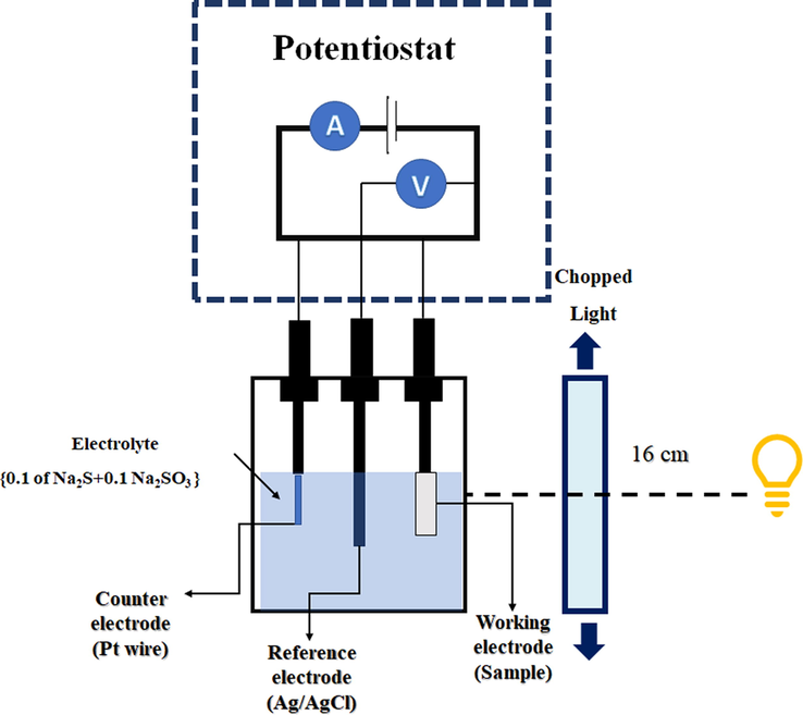
Setup for photoelectrochemical configuration cell.
2.4 Characterisation
Field emission scanning electron microscope (FE-SEM, JEOL JSM-7600F) was used to analysis the morphology structure of the nanocomposite thin films. The crystal structure was determined by X-ray diffractometer Philips PM1730 diffractometer (Panalytical X’Pert Pro MPD diffractometer) using a Cu-Kα (λ = 1.54 Å) radiation of 40 kV and 40 mA under a scanning speed of 5°/min in a range of 10° < 2θ < 80° equipped with Panalytical Xpert Highscore software. UV–Vis spectrophotometer (UV-2600, Shimadzu) in the wavelength range between 300 and 800 nm was used to study the optical characteristics of the synthesised samples for which plain ITO substrate was used as a reference. While the high-resolution transmission electron microscopy (HR-TEM) with selected area electron diffraction (SAED) and electron energy-loss spectroscopy (EELS) modes in Tecnai TF20 x-twin FEI system were used to examine the nature of the crystalline phase, lattice fringe, and chemical composition of the optimum ternary photoanode, respectively. The XPS study was done using an X-ray photoelectron spectroscopy (XPS) (ULVAC-PHI Quantera II) equipped with Al K-Alpha Monochromatic Source (1486.6 eV) and X-ray beam size of 100 µm.
3 Results and discussion
Fig. 2 displays the representative top view FESEM images of as-fabricated ZnO NRAs, Bi2S3/ZnO NRAs/ITO, Ag2S/ZnO NRAs/ITO and Bi2S3/Ag2S/ZnO NRAs/ITO photoanodes. From this figure, it can be noticed that ZnO NRAs were well-aligned in vertical orientation and with uniformly grown structure on the ITO substrate. The diameter of the ZnO NRAs was determined to be ∼37 ± 2 nm with an aspect ratio of about 20.45. The vertical grown ZnO NRAs were expected to provide a large surface area for the deposition of Ag2S and Bi2S3 nanoparticles. It can be seen that the decoration of ZnO NRAs with Bi2S3 and Ag2S did not drastically change the morphological structure of ZnO NRAs as they were homogenously coated on the ZnO NRAs as shown in Fig. 2(c-h). However, the surface of ZnO NRAs became rougher after the deposition of both metal chalcogenides. These structures and morphologies of the fabricated thin films would substantially influence the light penetration during the photoelectrochemical performance.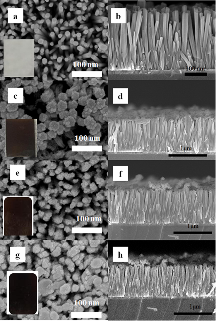
Plane view FESEM images with cross-sectional of: (a-b) bare ZnO NRAs; (c-d) Bi2S3/ZnO NRAs/ITO; (e-f) Ag2S/ZnO NRAs/ITO; (g-h) Bi2S3/Ag2S/ZnO NRAs/ITO.
Fig. 3 shows the FESEM images of Bi2S3/Ag2S/ZnO NRAs/ITO the effect of post-heat treatment at different annealing temperature. Based on the FESEM results, it was found that the average particle sizes of Bi2S3/Ag2S/ZnO NRAs/ITO increased with increasing annealing temperature as listed in Table 1. The increment of particle size in the film may be attributed to the sintering of small nanoparticles during the annealing process. The elevated heat at higher temperature caused a massive expansion of small nanoparticles that clogged the spaces between the ZnO nanorods (Lu et al., 2010).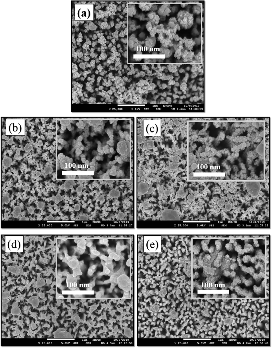
FESEM images of Bi2S3/Ag2S/ZnO NRAs/ITO electrode synthesized at different annealing temperatures: (a) as-deposited; (b) 100 °C; (c) 200 °C; (d) 400 °C; (e) 500 °C.
Annealing temperature (°C)
Particle size (nm)
As-deposited
104
100
139.53
200
156.49
300
239.43
400
245.58
500
280.13
Fig. 4 displays the XRD patterns of ITO conductive glass, ZnO NRAs, and Bi2S3/Ag2S/ZnO NRAs/ITO thin films treated thermally between 100 °C and 500 °C. The XRD patterns revealed that the hydrothermally synthesised ZnO NRAs were well crystallised in hexagonal wurtzite phase (JCPDS No. 00-003-0888) with a strong orientation along the (0 0 2) plane on the ITO glass at 2θ = 34.7° (Narayanan et al., 2016). The other diffraction peaks of ZnO NRAs are (1 0 0), (1 0 1), (1 0 2), (1 1 0), (1 0 3), and (1 1 2) planes, located at 2θ of 31.77°, 36.25°, 47.56°, 56.60°, 62.86°, and 67.96°, respectively. After Ag2S and Bi2S3 deposition on the ZnO NRAs, more main peaks appeared as located at 22.4°, 28.65°, 32.92°, 33.98°, 53.79°, and 73.21° corresponding to the (0 2 2), (0 2 3), (1 3 0), (1 1 3), (1 0 6), and (3 0 2) planes, respectively. The overlapping peaks over ZnO at 2θ = 34.7°, 36.21°, 72.72° are attributed to the orthorhombic structure of Bi2S3 (JCPDS card No. 03-065-3884). The other distinct peaks located at 36.56°, 37.2°, 37.8°, and 53.3° are attributed to (1 1 2), (0 1 3), (
, respectively, of the monoclinic structure of Ag2S (JCPDS 00-014-0072). The diffraction peaks of Bi2S3 and Ag2S were relatively weak in comparison to those of ZnO due to the growth of the (0 0 2) lattice plane along the [0 0 1] direction of that ZnO nanorod over Bi2S3 or Ag2S. In particular, some diffraction peaks such as (0 2 3), (0 5 2), (1 2 6), (1 7 2) and (1 2 8) at 2θ° = 28. 65, 43.61, 56.8, 65.2, 73.1, respectively are seen to exhibit high intensity with increasing temperature but then started declining after 400 °C. There were no traces of other impurities peaks detected, verifying the purity of the ternary nanocomposite structure. These observations are in agreement with FESEM images presented earlier.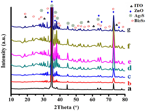
XRD diffractogram of: (a) ZnO NRAs/ITO; Bi2S3/Ag2S/ZnO NRAs/ITO prepared at different annealing temperatures: (b) as-deposited; (c) 100 °C; (d) 200 °C; (e) 300 °C; (f) 400 °C; (g) 500 °C.
The absorption spectra of ZnO NRAs before and after deposition of Ag2S and Bi2S3 as well as the heat-treatment are shown in Fig. 5A. The absorption edge of the bare ZnO NRAs occurred at 385.09 nm, corresponding to its band gap energy of 3.22 eV. On the other hand, the absorption of as-deposited Bi2S3/Ag2S/ZnO NRAs/ITO were extended to 596.15 nm before the heat-treatment. Upon annealing, the absorbance edge showed a red-shifted behaviour with absorption edges of 656.08 nm, 692.73 nm, 733.73 nm, 775 nm, and 794.87 nm for samples treated at 100 °C, 200 °C, 300 °C, 400 °C, and 500 °C, respectively. Following this, the band gap energy was estimated using the Tauc’s plot which corresponds to the relationship between the energy of the photon (hv) and absorption coefficient (α) as shown in Eq. (1) (Tauc et al., 1966):
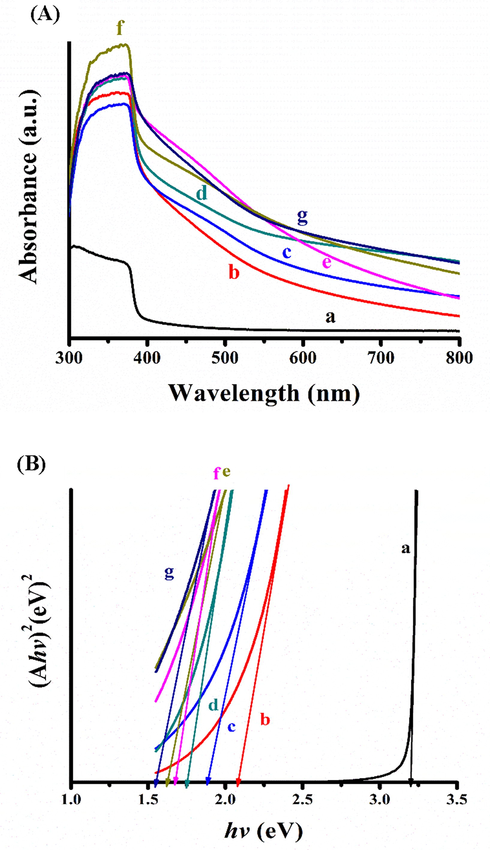
(A) UV–Vis spectra; (B) bandgap energy curves of: (a) ZnO NRAs/ITO; (b) Bi2S3/Ag2S/ZnO NRAs/ITO-as deposited; (c) 100 °C; (d) 200 °C; (e) 300 °C; (f) 400 °C; (g) 500 °C.
Table 2 listed the optical band gap energy values at different annealing temperatures. Interestingly, increasing the annealing temperature led to a systemic reduction of the band gap energy based on Fig. 5B. The Eg of annealed samples at 100 °C, 200 °C, 300 °C, 400 °C, and 500 °C reduced to 1.89 eV, 1.79 eV, 1.69 eV, 1.60 eV, and 1.56 eV, respectively. This reduction of band gap energy with increasing temperature can be attributed to the continuous growth of the nanocrystal while removing the grain boundaries which allows better penetration of light to the photoanode (Holi et al., 2018).
Photoanodes
Eg (eV)
ZnO NRAs/ITO-as deposited
3.22
Ag2S/ZnO NRAs/ITO-as deposited
2.23
Bi2S3/Ag2S/ZnO NRAs/ITO as deposited
2.08
Bi2S3/Ag2S/ZnO NRAs/ITO-100 °C
1.89
Bi2S3/Ag2S/ZnO NRAs/ITO 200 °C
1.79
Bi2S3/Ag2S/ZnO NRAs/ITO 300 °C
1.69
Bi2S3/Ag2S/ZnO NRAs/ITO 400 °C
1.60
Bi2S3/Ag2S/ZnO NRAs/ITO 500 °C
1.56
The Bi2S3/Ag2S/ZnO NRAs/ITO annealed at different temperatures were applied in the PEC cell to assess the performance in the dark condition and under simulated solar illumination (100 mW/cm2) based on the reversible hydrogen electrode (RHE) equation. Fig. 6 shows the photocurrent density versus the applied potential characteristics of ZnO NRAs, Bi2S3/ZnO NRAs/ITO, Ag2S/ZnO NRAs/ITO, and Bi2S3/Ag2S/ZnO NRAs/ITO with chopping under simulated light illumination as plotted using Eq. (2).
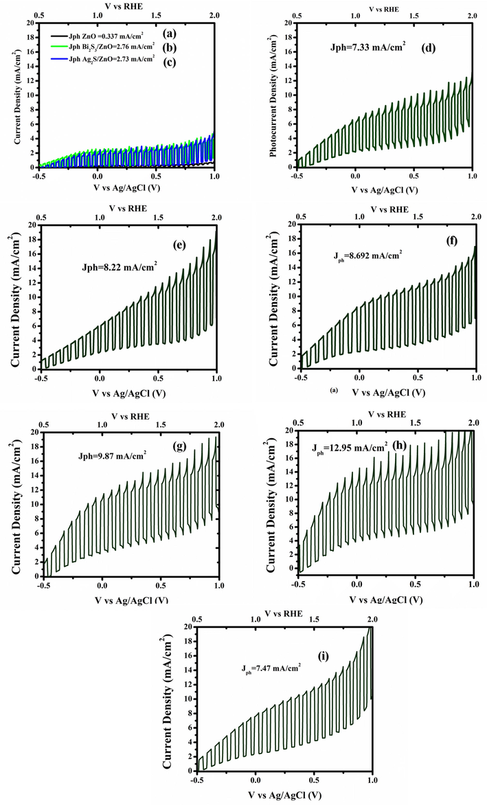
Linear sweep voltammograms obtained at the scan rate of 20 mV s−1 at applied potentials range from −0.5 V to +1.0 V under illumination intensity of 100 mWcm−2 in 0.1 M Na2S and Na2SO3 electrolyte for: (a) pure ZnO NRAs/ITO; (b) Ag2S/ZnO NRAs/ITO; (c) Bi2S3/ZnO NRAs/ITO/ and Bi2S3/Ag2S/ZnO NRAs/ITO at different annealing temperatures: (d) as-deposited; (e) 100 °C; (f) 200 °C; (g) 300 °C; (h) 400 °C; (i) 500 °C.
The current–voltage profile at the bias voltage of +0.5 V revealed that the photocurrent density of the as-deposited ZnO NRAs, Ag2S/ZnO NRAs/ITO, and Bi2S3/Ag2S/ZnO NRAs/ITO were 0.337 mA/cm2, 2.73 mA/cm2, and 7.33 mA/cm2, respectively. The obtained data suggest that the separation of the photogenerated electrons is less effective in single and binary photoanodes as compared to the ternary heterostructure. Upon annealing, the PEC performance improved remarkably as the photocurrent density increased from 8.22 mA/cm2 at 100 °C until it reached the highest value of 12.95 mA/cm2 at 400 °C. It has been suggested that improving the film's crystallinity with improved absorbance property and minimizing the recombination centres could induce better separation of the electron-hole, leading to an increase in the photocurrent produced. Moreover, the post-heat treatment can decrease the defects within the thin film as a result of decreasing number of grain boundaries within the ternary heterostructure (Patil et al., 2020). Consequently, the recombination centres in the annealed samples reduced efficiently leading to enhanced photocurrent produced (Lu et al., 2010). However, the photocurrent dropped drastically to 7.47 mA/cm2 when the annealing temperature was increased to 500 °C. This remarkable reduction in the photocurrent density can be attributed to poor crystallinity of the photoanode at this particular annealing temperature as proven via FESEM image (Fig. 3e). Based on the LSV analysis, the Bi2S3/Ag2S/ZnO NRAs/ITO annealed at 400 °C was chosen as the optimum annealing temperature for the next characterisation.
Additional information on the optimum fabricated nanocomposite thin film is obtained via high resolution transmission electron microscopy (HR-TEM). Fig. 7(a) shows that the surface of unmodified ZnO rod was significantly smooth. On the other hand, successful deposition of Bi2S3/Ag2S on the ZnO NRAs via SILAR technique can be seen as portrayed by small nanoparticles of Ag2S and Bi2S3/Ag2S with average size of 10.88 nm and 20.88 nm, respectively attached on the ZnO rod in Fig. 7(b,c). The surface of the ZnO NRAs also seems coarser after the deposition of Bi2S3 and Ag2S nanoparticles. HR-TEM image and SAED pattern of Bi2S3/Ag2S/ZnO NRAs/ITO annealed at 400 °C is shown in Fig. 7(d, e). From Fig. 7(d), the existence of three sets of lattice fringes of ZnO NRAs, Ag2S, and Bi2S3 is noted using fast fourier transform (FFT). Specifically, Fig. 7(e) shows the ternary heterostructure exhibits polycrystalline nature where many diffraction spots of Bi2S3/Ag2S/ZnO NRAs/ITO were identified with d-spacing of 0.260, 0.238, and 0.310 nm in relation to (0 0 2), (
), and (0 2 3) planes of ZnO NRAs, Ag2S, and Bi2S3, respectively. Therefore, these results further confirmed that the Ag2S and Bi2S3 nanoparticles were deposited successfully without affecting the crystalline phase of the ZnO NRAs.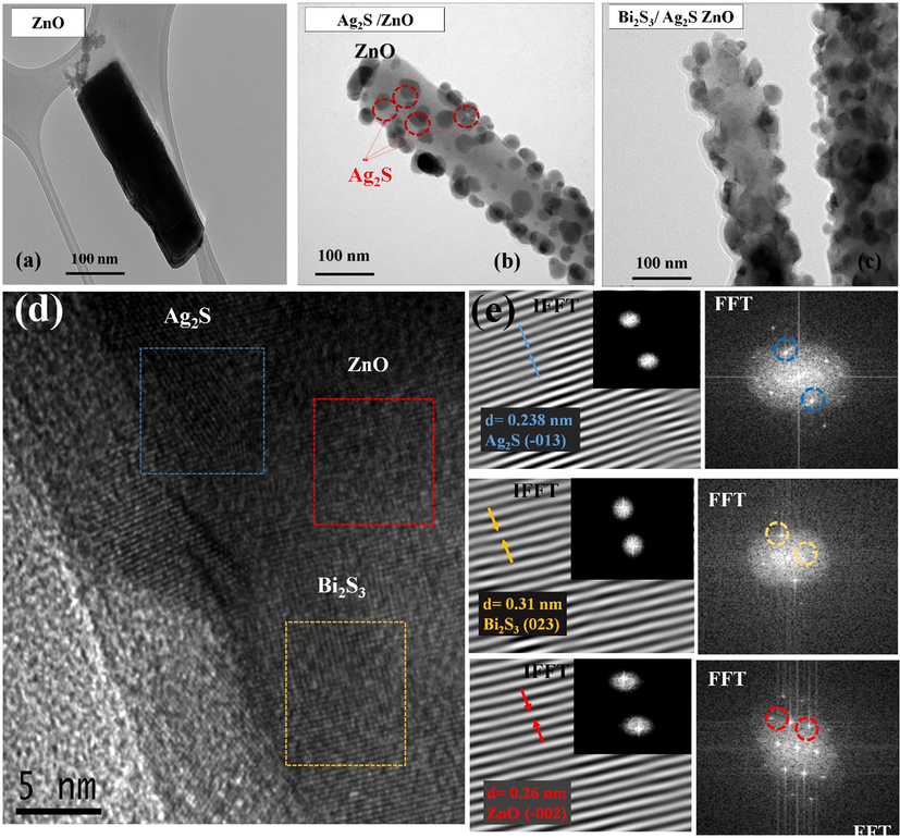
HR-TEM image of the optimum Bi2S3/Ag2S/ZnO NRAs/ITO annealed at 400 °C.
Chemical elemental mapping (EELS) as clarified with EDS of the nanocomposite measurements was performed on Bi2S3/Ag2S/ZnO NRAs/ITO under an optimal annealing temperature of 400 °C. In, Zn, O, Bi, Ag, and S elements were detected in the wide survey scan, as displayed in Fig. 8 in which In refers to indium element from the ITO glass. The atomic weight percentage (Wt%) based on EDX result of Zn, O, Bi, Ag, and S were 52.53%, 25.19%, 9.73%, 6.40%, and 6.21%, respectively.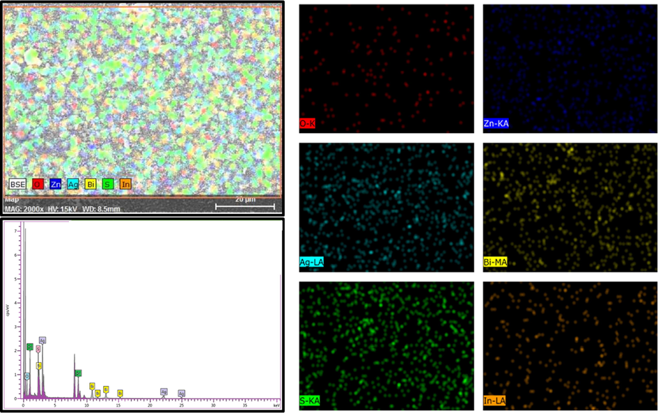
EDS pattern and elemental mapping (EELS) of Bi2S3/Ag2S/ZnO NRAs/ITO annealed at 400 °C.
Quantitatively, the surface chemistry, binding energy and oxidation states of Bi2S3/Ag2S/ZnO NRAs/ITO annealed at 400 °C was examined using XPS analysis in Fig. 9. The distinct peaks of Zn, O, Bi, S, Ag, and S elements were detected without the presence of any other impurities. The binding energy at 284.60 eV belongs to the C 1s transition (Balachandran and Swaminathan, 2013) and was made as a reference for the binding energy of other elements in the ternary heterostructure. The high-resolution XPS peak for Zn 2p binding energy is shown in Fig. 10(a). The Zn 2p binding energy peak was split into Zn 2p3/2 and Zn 2p1/2 peaks as a result of spin-orbital coupling situated at 1022.37 eV and 1045.49 eV, respectively. Furthermore, the spin-orbital separation with energy equals to 23.12 eV, verified that Zn (II) oxidation state existed in hexagonal wurtzite structure (Majumder et al., 2018; Al-Gaashani et al., 2013). Fig. 10(b) represents the narrow survey of XPS spectra with O1s binding energy. The O1s broad peak was deconvoluted into three peaks located at 530.07 eV, 531.42, and 532.83 eV. The peak located at 530.07 eV was assigned to the oxygen ions in the hexagonal wurtzite of ZnO whereas the peak at 531.42 eV confirmed the existence of O2 in O-H bond (Nesheva et al., 2018). Meanwhile, the peak located at 532.83 eV might be attributed to chemisorbed oxygen as reported by Alshehri et al. (Alshehri et al., 2018). On the other hand, the binding energies located at 158.00 eV and 163.30 eV as shown in Fig. 10(c) were due to Bi 4f7/2 and Bi4f5/2, respectively indicating the presence of Bi (III) in the ternary structure. The mentioned peaks are in a good agreement with other reported work (Helal et al., 2017). The two binding energy peaks located between the Bi binding energy were attributed to the S 2p spectrum separated into the S2p3/2 and S2p1/2 peaks as observed at 160.84 eV and 162.00 eV binding energy, respectively (Balachandran and Swaminathan, 2013). This verifies significantly the existence of S2p anions coordinated to Bi3+ in the Bi2S3/Ag2S/ZnO NRAs/ITO ternary heterostructure.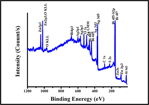
The XPS survey spectra of optimal Bi2S3/Ag2S/ZnO/ITO sample.
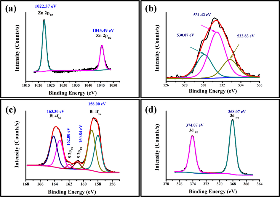
XPS spectra of Bi2S3/Ag2S/ZnO NRAs/ITO heterostructure (optimal sample annealed at 400 °C): (a) Zn 2p spectra; (b) O 1s spectra; (c) Bi 4f and S 2p spectra; (d) Ag 3d spectra.
Meanwhile, Fig. 10(d) shows that the Ag 3d5/2 and Ag 3d3/2 peaks were found at 368.09 and 374.07 eV, respectively, suggesting that the oxidation state of silver was bivalent Ag2+ in the ternary thin film (Shi et al., 2019; Ruiz et al., 2019). Ultimately, these outcomes further verify the synthesised photoanodes were comprised of ZnO, Ag2S and Bi2S3.
In order to better understand the dynamics of the electrochemical and PEC processes occurring in the photoelectrodes, the EIS analysis of the photoelectrodes is performed. The EIS measurements of photoelectrode are conducted using similar polysulfide electrolyte. Fig. 11 shows the Nyquist plot for the PEC performance of ZnO NRAs, Ag2S/ZnO NRAs, Bi2S3/Ag2S/ZnO electrodes before and after annealing at 400 °C. The charge transfer resistance at semiconductor/electrolyte (Rct) is determined based on Nyquist plot. It can be clearly observed that the diameter of semicircles of the annealed Bi2S3/Ag2S/ZnO NRAs photoelectrode is smaller than that of the plain ZnO, Ag2S/ZnO NRAs, Bi2S3/Ag2S/ZnO before annealing. The Rct for as-prepared ZnO NRAs, Ag2S/ZnO, Bi2S3/Ag2S/ZnO are 12232.55, 9672.80 and 6668.49 Ω/cm2, respectively whereas after annealing, the Rct of Bi2S3/Ag2S/ZnO is 3857.79 Ω/cm2. This means the resistance of thermally treated Bi2S3/Ag2S/ZnO photoelectrode is smaller, which can greatly and effectively improve the separation of photo-generated electron–hole pairs.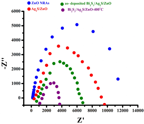
Nyquist Plots (Real Z vs imaginary Z) of plain ZnO NRAs; Ag2S/ZnO NRAs; as-deposited Bi2S3/Ag2S/ZnO NRAs/ITO and Bi2S3/Ag2S/ZnO NRAs/ITO annealed at 400 °C.
The PEC characteristics of the fabricated ternary thin films were further evaluated by calculating the photoconversion efficiency (η%) using Eq. (3) (Rattanawarinchai et al., 2018):
Photoanodes
Photoconversion efficiency, η (%)
ZnO NRAs/ITO-as deposited
0.25%
Ag2S/ZnO NRAs/ITO-as deposited
1.65%
Bi2S3/Ag2S/ZnO NRAs/ITO -as deposited
7.64%
Bi2S3/Ag2S/ZnO NRAs/ITO −100 °C
8.44%
Bi2S3/Ag2S/ZnO NRAs/ITO −200 °C
8.50%
Bi2S3/Ag2S/ZnO NRAs/ITO −300 °C
10.22%
Bi2S3/Ag2S/ZnO NRAs/ITO −400 °C
12.63%
Bi2S3/Ag2S/ZnO NRAs/ITO −500 °C
5.64%
Thus, Bi2S3 and Ag2S co-sensitisation can effectively enhance the PEC performance due to effective cascade band gap alignment. The electrons in the valence bands of Bi2S3, Ag2S, and ZnO are excited to (C.B.) of Bi2S3, Ag2S, and ZnO under illumination. Then, the photogenerated electrons in the C.B. of Bi2S3 with a more negative potential energy (−0.82 V) transfer to the C.B of Ag2S (−0.43 V) and then to the C.B. of ZnO (−0.32 V). At the same time, the photogenerated holes accumulated in ZnO with a more positive potential energy (2.9 V) migrate to Ag2S (1.35 V) and then to Bi2S3 (0.82 V). The photoinduced electrons and holes accumulated at ZnO’s C.B. and Bi2S3’s V.B. promoting effective separation of photoinduced charge carriers as a result of a stepwise band alignment of Bi2S3/Ag2S/ZnO NRAs/ITO heterostructure. The heterojunction architecture allows more incoming light and increases the separation of the charge. Additionally, introducing Ag2S as a medium layer between ZnO and Bi2S3 nanoparticles acted as a highway bath of photogenerated electrons and holes facilitating efficient charge transfer process as shown in Fig. 12 (Ye et al., 2019).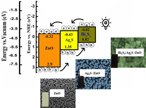
Relative energy levels and ideal cascade band structure in Bi2S3/Ag2S/ZnO NRAs/ITO heterostructure ternary system.
4 Conclusion
In summary, the hydrothermal ZnO NRAs were successfully sensitised using Ag2S and Bi2S3 as a ternary nanocomposite heterostructure Bi2S3/Ag2S/ZnO NRAs/ITO for PEC application. The effect of the annealing process was pronounced as the performance of the ternary photoanode was two times greater than without heat treatment. The Bi2S3/Ag2S/ZnO NRAs/ITO nanocomposites annealed at 400 °C showed a significant enhancement on photocurrent density with 12.95 mA/cm2, which was 38 times superior than plain ZnO NRAs (0.337 mA/cm2) and almost 5 times greater than the binary photoanode Ag2S/ZnO NRAs/ITO (2.73 mA/cm2). The thermally treated Bi2S3/Ag2S/ZnO NRAs/ITO photoanode exhibited improved crystallinity, which allowed better visible light absorption for electron-hole excitation. The cascade band gap alignment of the ternary system further facilitated the separation of the photogenerated charge carriers for enhancement of PEC performance.
Acknowledgments
The author would like to thank Universiti Putra Malaysia for providing the facilities and equipment required for this study. Special thanks are extended to the Ministry of Higher Education of Malaysia for financial support via FRGS grant (01-01-17-1912FR). Saudi culture mission is highly acknowledged for financial support to Asla Abdullah Al-Zahrani.
Declaration of Competing Interest
The authors declare that they have no known competing financial interests or personal relationships that could have appeared to influence the work reported in this paper.
References
- XPS and optical studies of different morphologies of ZnO nanostructures prepared by microwave methods. Ceram. Int.. 2013;39(3):2283-2292.
- [Google Scholar]
- Investigation of the growth parameters of hydrothermal ZnO nanowires for scale up applications. J. Saudi Chem. Soc.. 2018;22(5):538-545.
- [Google Scholar]
- Synthesis of binary Bi2S3/ZnO nanorod array heterostructure and their photoelectrochemical performance. J. Nanomater.. 2019;2019:1-10.
- [Google Scholar]
- Study the effect of the heat treatment on the photoelectrochemical performance of binary heterostructured photoanode Ag2S/ZnO nanorod arrays in photoelectrochemical cells. Mater. Sci. Forum. 2020;1002:187-199.
- [Google Scholar]
- The simple, template free synthesis of a Bi2S3–ZnO heterostructure and its superior photocatalytic activity under UV-A light. Dalt. Trans.. 2013;42:5338-5347.
- [Google Scholar]
- Extraction of ZnO thin film parameters for modeling a ZnO/Si solar cell. Energy. 2018;164
- [Google Scholar]
- Enhanced visible light photocatalytic performance of ZnO nanowires integrated with CdS and Ag 2 S. Dalt. Trans.. 2016;45(9):3750-3758.
- [Google Scholar]
- Ag2S/Bi2S3 co-sensitized TiO2 nanorod arrays prepared on conductive glass as a photoanode for solar cells. J. Mater. Sci. Mater. Electron.. 2016;27(4):3234-3239.
- [Google Scholar]
- Effect of structure morphologies on hydrogen gas sensing by ZnO nanotubes. Mater. Lett.. 2018;230:48-52.
- [Google Scholar]
- Hetero-seed meditated method to synthesize ZnO/TiO2 multipod nanostructures with ultra-high yield for dye-sensitized solar cells. J. Alloys Compd.. 2019;805:868-872.
- [Google Scholar]
- Hydrothermal synthesis of novel heterostructured Fe2O3/Bi2S3 nanorods with enhanced photocatalytic activity under visible light. Appl. Catal. B Environ.. 2017;213:18-27.
- [Google Scholar]
- Optimization of an electrode made from CdS-ZnO nanorods for hydrogen generation from photoelectrochemical splitting of water. Adv. Nat. Sci. Nanosci. Nanotechnol.. 2017;8(2):025006
- [Google Scholar]
- Effect of hydrothermal growth time on ZnO nanorod arrays photoelectrode performance. Optik (Stuttg). 2016;127(23):11111-11118.
- [Google Scholar]
- Enhanced photoelectrochemical performance of ZnO nanorod arrays decorated with CdS shell and Ag2S quantum dots. Superlattices Microstruct.. 2017;103:295-303.
- [Google Scholar]
- Effect of heat treatment on photoelectrochemical performance of hydrothermally synthesised Ag2S/ZnO nanorods arrays. Chem. Phys. Lett.. 2018;710(January):100-107.
- [Google Scholar]
- Controlled synthesis and understanding of growth mechanism – parameters for atmospheric pressure hydrothermal synthesis of ultrathin secondary ZnO nanowires. J. Sci. Res. Reports. 2016;9(5):1-10.
- [Google Scholar]
- Zinc oxide-from synthesis to application: A review. Materials (Basel). 2014;7(4):2833-2881.
- [Google Scholar]
- Bismuth sulfide (Bi2S3) nanotubes decorated TiO2 nanoparticles heterojunction assembly for enhanced solar light driven photocatalytic activity. Ceram. Int.. 2016;42(15):17551-17557.
- [Google Scholar]
- Effects of annealing conditions on the photoelectrochemical properties of dye-sensitized solar cells made with ZnO nanoparticles. Sol. Energy. 2010;84(5):844-853.
- [Google Scholar]
- Advantages of ZnO nanotaper photoanodes in photoelectrochemical cells and graphene quantum dot sensitized solar cell applications. J. Electroanal. Chem.. 2018;813(February):92-101.
- [Google Scholar]
- Hierarchically assembled ZnO nanocrystallites for high-efficiency dye-sensitized solar cells. Angew. Chem. Int. Ed. 2011;50(51):12321-12325.
- [Google Scholar]
- Effect of temperature and growth time on vertically aligned ZnO nanorods by simplified hydrothermal technique for photoelectrochemical cells. Materials (Basel). 2018;11(5):704.
- [Google Scholar]
- Effect of annealing temperature on structural, optical and electrical properties of hydrothermal assisted zinc oxide nanorods. Thin Solid Films. 2016;598(3):39-45.
- [Google Scholar]
- Surface modification and chemical sensitivity of sol gel deposited nanocrystalline ZnO films. Mater. Chem. Phys.. 2018;209:165-171.
- [Google Scholar]
- CdS surface encapsulated ZnO nanorods: Synthesis to solar cell application. J. Alloys Compd.. 2016;689:394-400.
- [Google Scholar]
- SILAR controlled CdSe nanoparticles sensitized ZnO nanorods photoanode for solar cell application: Electrolyte effect. J. Colloid Interface Sci.. 2018;524:148-155.
- [Google Scholar]
- ZnO devices and applications: A review of current status and future prospects. Proc. IEEE. 2010;98(7):1255-1268.
- [Google Scholar]
- Facile designing and assessment of photovoltaic performance of hydrothermally grown kesterite Cu2ZnSnS4 thin films: Influence of deposition time. Sol. Energy. 2020;201(February):102-115.
- [Google Scholar]
- Investigating the role of selenium-ion concentration on optoelectronic properties of the Cu2ZnSn(S1- xSex)4 thin films. Ind. Eng. Chem. Res.. 2020;59(23):10868-10881.
- [Google Scholar]
- Growth time dependence on photoelectrochemical property of ZnO nanorods prepared by hydrothermal synthesis. Surf. Rev. Lett.. 2018;25(Supp01):1840001.
- [Google Scholar]
- Synthesis and characterization of Ag2S and Ag2S/Ag2(S, Se) NIR nanocrystals. Nanoscale. 2019;11(18):9194-9200.
- [Google Scholar]
- Fabrication of Ag2S quantum dots sensitized CdSe photoelectrodes and its photoelectric performance. Mater. Chem. Phys.. 2019;240(July 2019):122177.
- [Google Scholar]
- Optical properties and electronic structure of amorphous germanium. Phys. Stat. Sol.. 1966;15(2):627-637.
- [Google Scholar]
- Cascade structured ZnO/TiO2/CdS quantum dot sensitized solar cell. Solid State Sci.. 2020;102(February):106176.
- [Google Scholar]
- Structure optimization on the photoelectric and photocatalytic properties of Cu2S and ZnO complex films. Mater. Today Proc.. 2015;2(1):253-260.
- [Google Scholar]
- Recent advances in synthetic methods and applications of Ag2S-based heterostructure photocatalysts. J. Mater. Chem. C. 2019;7(14):3988-4003.
- [Google Scholar]
- Improving the performance of PbS quantum dot solar cells by optimizing ZnO window layer. Nano-Micro Lett.. 2017;9(2)
- [Google Scholar]
- An ultrathin carbon layer activated CeO2 heterojunction nanorods for photocatalytic degradation of organic pollutants. Appl. Catal. B Environ.. 2019;259(June)
- [Google Scholar]
- A novel CoOOH/(Ti, C)-Fe2O3 nanorod photoanode for photoelectrochemical water splitting. Sci. China Mater.. 2018;61(6):887-894.
- [Google Scholar]
- Photoelectrochemical properties of electrochemically deposited metal chalcogenide/ZnO films. Appl. Surf. Sci.. 2015;350:87-93.
- [Google Scholar]
- Photoelectrochemical properties of Bi2S3 thin films deposited by successive ionic layer adsorption and reaction (SILAR) method. Mater. Lett.. 2017;199:188-191.
- [Google Scholar]