

Translate this page into:
Selective electrochemical etching of the Sn-3Ag-0.5Cu/0.07 wt% graphene nanoparticle composite solder
⁎Corresponding author. aam@usm.my (Ahmad Azmin Mohamad)
-
Received: ,
Accepted: ,
This article was originally published by Elsevier and was migrated to Scientific Scholar after the change of Publisher.
Abstract
The morphological changes of SAC305 solder alloy with the addition of 0.07 wt% graphene was investigated using selective electrochemical etching. To evaluate the effect of graphene inclusion, selective electrochemical removal of the β-Sn phase from SAC305 and SAC305/0.07GNP was performed using a standard three-electrode cell approach at specific potentials determined by cyclic voltammetry. The phase, chemical structure and microstructural changes were observed. The texture and the phases of SAC305 solder paste were retained, while the microstructure of β-Sn and Ag3Sn was refined owning to graphene addition. Sufficient removal of β-Sn without affecting other phases was obtained by using etching potential below −350 mV. Due to Van der Waals force attraction, two types of agglomeration of graphene were observed from cross-sectional observation. Large agglomerations seen at the vicinity of solder/substrate interface were found to help in forming diffusion barrier. This contributes to the refinement of microstructure with the presence of graphene. Accurate observation regarding the shape and texture of the intermetallic compound (IMC) phases affected by the addition of graphene provided by selective electrochemical removal helps better insight into understanding the electrochemical dissolution mechanism of SAC alloys.
Keywords
Lead-free solders
Sn-3.0Ag-0.5Cu
Selective electrochemical etching
Microstructure
Graphene
Composite solder

1 Introduction
The ternary Sn-Ag-Cu (SAC) series alloy was recognized as one of the most suitable candidates to replace Sn-Pb alloys due to its comparable melting characteristic and mechanical properties. The SAC series, particularly Sn-3Ag-0.5Cu (SAC305), were also the most commercially used Pb-free solders in the current electronic industries (Lee and Mohamad, 2013; Nimmo, 2002). Despite its promising properties, the reliability of SAC solder alloys is still a concern due to the presence of brittle intermetallic compound (IMC) in its microstructure, leading to a drawback in mechanical performance. The sizes and shapes of IMCs in SAC had a great influence on hardness (Chellvarajoo et al., 2015), shear strength (Han et al., 2012), creep resistance (El-Daly et al., 2014) and tensile strength (Sharma et al., 2016). Various works on SAC solder alloys proved that the sizes and shapes of IMC can be altered by the adding alloying element and fine second phase reinforcing materials. The latter method had gained high interest since it can avoid modification to melting characteristic that has been well established in SAC alloy series.
Graphene has attracted the attention of many researchers due to its superb and unique characteristics. Due to its two-dimensional structure, graphene possessed remarkable properties in term of biocompatibility (Syama and Mohanan, 2016), electrical conductivity (Chen et al., 2008), thermal properties (Balandin et al., 2008) and optical properties (Falkovsky, 2008). In composite solder studies, graphene had been recognized as a promising reinforcement material due to its excellent mechanical and electrical properties. Several works on graphene reinforcement to SAC solders had proved that the addition of graphene improved the mechanical properties of the solder in terms of ultimate tensile strength (UTS) (Liu et al., 2013), wettability (Huang et al., 2016), microhardness (Sharma et al., 2016), and shear strength (Chen et al., 2016a, 2016b). The presence of passive nanoparticles such as graphene exerted pressure that halted the grain boundaries movement. This phenomenon known as the Zener pinning helped in improving the physical and mechanical properties of solders (Kotadia et al., 2012, Mokhtari et al., 2012).
The variant of graphene reinforcements has been used in the form of 0.01 to 0.1 wt% graphene nanoparticles (GNP) (Sharma et al., 2016), 0.03 to 0.1 wt% graphene nanosheets (GNS) (Liu et al., 2013), 0.02 to 0.1 wt% GNS (Huang et al., 2016), and 0.05 to 0.2 wt% GNS) (Chen et al., 2016a, 2016b). Although the studies of graphene reinforced SAC solder have showed the positive impact on solder properties especially at the additions of 0.05 to 0.1 wt%, it is expected that the properties of composite solder can be further improved if an in-depth understanding on the reinforcement mechanism is obtained. The in-depth understanding on the reinforcement mechanism, especially by graphene can be achieved via advanced characterization techniques, which gives more insight on the structure and microstructure of the composite solder.
The development of novel electrochemical etching technique of SAC solder gives us promising motivation to obtain a clearer insight on the microstructure of SAC composite solder (Hurtony et al., 2012). This study showed that a detailed microstructure of SAC solder can be obtained by applying a potential bias to an electrochemical cell with the SAC solder as a working electrode. However, since this etching technique is still in the development stages, the electrochemical dissolution mechanism of SAC alloys still remains to be understood. The understanding on the dissolution mechanism will enable us to justify the selection of correct potential bias to be used during electrochemical etching to avoid over etching of IMC structure, even further in the composite solder.
In this work, the data and analysis on the effectiveness of selective electrochemical etching on morphological observation of SAC305 and SAC305-0.07 wt% GNP (SAC305-0.07GNP) composite solder are presented. The presentation can be categorized into two parts. The first part includes the preparation and basic characterizations of SAC305 solder and SAC305-0.07GNP composite solder, involving phase and chemical structure changes. The second part is selective electrochemical etching by cyclic voltammetry (CV) and morphological observation of SAC305 solder and SAC305-0.07GNP composite solder.
2 Experimental
2.1 Sample preparation
The SAC305 solder alloy paste (ALPHA OM-353, Alpha Assembly Solutions) was used in this work. The SAC305 solder paste, and 0.07 wt% graphene nanoparticles (11–15 nm, Skyspring Nanomaterial Inc) were mixed using planetary ball mill (Pulverisette 5, Fritsch). The ball milling speed and time were set at 300 rpm and 10 min, respectively. The selection of optimum milling speed and time is crucial to ensure homogeneity of graphene distribution in the solder as well as the retaining of paste-like properties of the SAC305 solder paste.
The SAC305 and SAC305-0.07GNP composite solder pastes were printed onto a 2 cm × 3 cm FR4 substrate (Density Electronics) by a custom stencil. This is followed by reflowing in a conventional reflow oven (T200N, Beijing Torch Co. Ltd) in with a programmed reflow profile: preheating (160–180 °C), reflowing (213–247 °C), and cooling (247–40 °C).
The reflowed solder samples related to copper wire (Density Electronics) by soldering. The overall length of the wire for all samples was maintained at 15 mm to ensure uniform electrical resistivity. The solder samples were mounted in epoxy resin to allow easier handling and to control the exposure area. Finally, grinding and polishing were performed on the solder surface until mirror images are achieved. The grinding process was done with 800, 1200, and 2000 grit silicon carbide papers and the polishing process was performed using 1.0, 0.5, and 0.03 µm alumina suspensions. Diamond cutter (MIRACUT, Metcon) was used to cut the samples prior to mounting in epoxy resin. The mounting process allows easier handling and provides exposure only on the specified area of the composite solder.
2.2 Sample characterizations
2.2.1 Electrochemical characterization
Electrochemical characterizations were conducted on SAC305 solder samples to study the electrochemical dissolution mechanism. Three electrode configurations with 1 % sulfuric acid were used for all electrochemical characterizations (cyclic voltammetry (CV) and chronoamperometry (CA)). The setup for the electrochemical cell consists of SAC305 solders (working electrode), platinum rod (counter electrode), and a saturated calomel electrode (reference electrode, Koslow), electrodes were kept 1 cm away from each other. The electrolyte was changed after every test to ensure its freshness. Scan rate of 0.1 mVs−1 was used for CV, based on our previous study (Ahmad et al., 2019). For selective electrochemical etching, CA was done at − 350 mV for 240 s for every sample. All electrochemical evaluations were conducted using potentiostat/galvanostat (Autolab, PGSTAT101) with NOVA 10 software and was repeated at least three times to ensure reproducibility of the results.
2.2.2 Phase identification
Phase analysis was used to observe the reduction of Sn in the samples due to electrochemical dissolution of SAC305, and the phase changes of SAC305/0.07GNP composite solder. The analysis was conducted on the solder samples using X-ray diffraction (XRD, Bruker AXS D8 Advance) with monochromatized Cu Kα radiation (λ = 1.5406 A). The diffraction range was set as 10° < 2θ < 90°. Phase identification was also crucial in detecting the retainment of graphene reinforcement particles in the samples after reflowing.
2.2.3 Raman spectroscopy
For clearer identification of graphene retainment in the composite solder, Raman spectroscopy technique was used using Renishaw inVia Raman Microscope. The laser spot mode was used with spoon size of 1 µm. The spectral range was set using SynchroScan™ from 100 to 3200 cm−1.
2.2.4 Morphological observation
Morphological observation for CV characterization, was conducted using tabletop microscope scanning electron microscope (TM-SEM, Hitachi). For CA characterization, the morphological changes were observed using a field emission scanning electron microscope (FESEM, 35VP, Zeiss SupraTM) to obtain more detail and sharp images. In addition, energy dispersive X-ray spectroscopy (EDX, EDAX USA) with area scan mode was also carried out to determine the elements present during morphological observation.
3 Results and discussion
3.1 Sample after reflow observation
Optical observation was performed during sample preparation for pure and composite solders to evaluate the difference between both samples. It was observed that the composite solder paste retained the texture of pure solder paste after mixing through the ball milling method. This observation showed that the addition of 0.07 wt% of graphene did not alter the texture of the solder paste (Fig. 1a and d). The printing process for composite solder paste (Fig. 1e) also does not exhibit any significant difference compared to pure solder (Fig. 1b).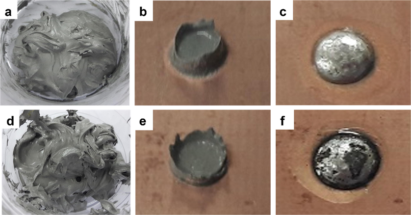
SAC305 (a) solder paste, (b) after printing, (c) after reflow, and SAC305/0.07GNP (d) after mixing by ball milling, (e) after printing, and (f) after reflow.
However, it was observed that the composite solder exhibits the appearance of black spots on top of the solder bump after reflowing (Fig. 1c and f). The appearance of these black spots could be caused by graphene expulsion during reflow process. Other researcher (Chen et al., 2016) reported that graphene can be expelled from the composite along with the flux during reflow process.
3.2 Phase identification
Phase analysis was performed on graphene, pure SAC305 and SAC305/0.07GNP composite solder to investigate the changes in the phase present in the composite solder after the addition of graphene as reinforcement. The XRD pattern obtained for graphene nanoparticle (ICDD 98–005-2931) exhibited a high intensity peak for (0 0 2) plane at 2θ of 26°, which is typical for multilayer graphene samples (Fig. 2a). A peak with significant intensity was also detected for (0 0 4) plane at 2θ of 54°. This pattern is in agreement with the results published in an extensive report for XRD (Seehra et al., 2017). The XRD pattern of the pure SAC305 sample showed the co-existence of β-Sn phases (ICDD 00–004-0673), Ag3Sn (ICDD 00–044-1300), and Cu6Sn5 (ICDD 00–045-1488), with the highest intensity peaks coming from the β-Sn phase (Fig. 2b).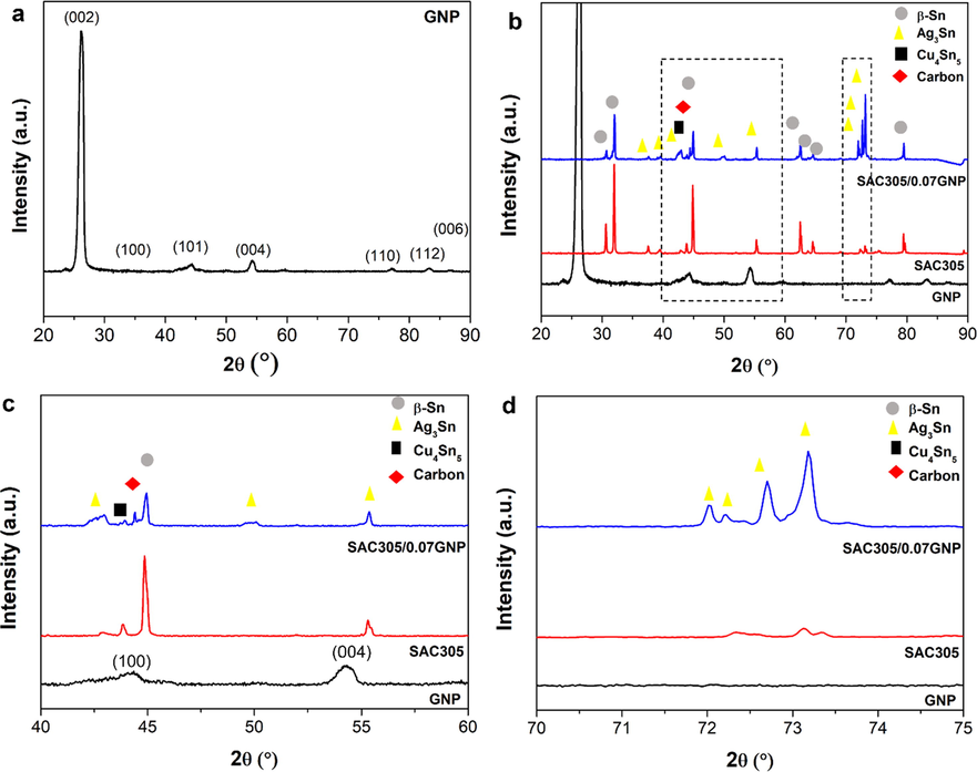
XRD pattern of (a) graphene nanopowder (GNP), XRD peaks of GNP, SAC305, and SAC305/0.07GNP at scanning (b) 20⁰ to 90⁰, (c) 40⁰ to 60⁰ and (d) 70⁰ to 75⁰.
One main peak of graphene corresponding to (1 0 1) plane was detected at 2θ of 44°, while most peaks were undetected (Fig. 2c). This observation signalled that graphene added to the solder is not entirely expelled during the reflow process. A small amount or graphene that left in the composite solder after reflow process. Overall, the intensity of Sn peaks does not show any significant changes upon addition of graphene (Fig. 2d). However, it is noticed that the intensity of Ag3Sn peaks in the range of 70°–75° has increased significantly (Fig. 2d). It is hypothesized that this is attributed to the refinement of Ag3Sn by the addition of graphene.
3.3 Raman spectroscopy
Raman spectroscopy characterization was performed to investigate the presence of graphene in SAC305/0.07GNP throughout the sample preparation process. Raman spectroscopy was performed on the GNP powder, SAC305/0.07GNP solder paste, and SAC305/0.07GNP solder after reflow process (Fig. 3a). A typical Raman spectrum of graphene was showed for GNP powder (black line). The Raman spectra consisted of D band peak at Raman shift of 1334.36 cm−1, G band peak at 1581.72 cm−1, and 2D peak at 2689.73 cm−1. The Raman spectra for SAC305/0.07GNP solder paste showed that the G band and 2D peak for graphene remained in the sample, indicating that graphene is present in solder paste. However, the D band peak for graphene is undetected in the Raman spectra for solder paste (red line). This is attributed to the ball milling process that enforces slipping of graphene layers (Zhao et al., 2010). The Raman spectra for the composite solder paste also exhibit unknown peaks (denoted as X and Y). This peak could be attributed to the flux materials in the solder paste.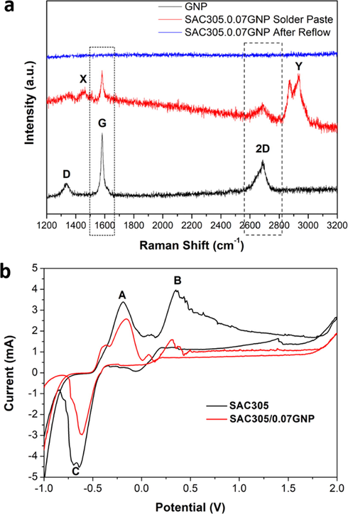
(a) Raman spectra of GNP, SAC305/0.07GNP solder paste, and SAC305/0.07GNP solder after reflow, and (b) CV peaks of SAC305 and SAC305/0.07GNP.
After the reflow process, it is observed that all the flux material and graphene peaks from the solder paste spectra were completely diminished (blue line). The disappearance of flux materials peak is attributed to the fluxing process during reflow that purged all the flux materials from the solder bump. Meanwhile, the disappearance of graphene peaks is due to the expulsion of graphene from the solder bump during the reflow process. Although an amount of graphene remained in the sample after reflowing as verified previously by the observation of (1 0 1) graphene plane in reflowed composite solder sample, this amount might be too low to be detected by a Raman spectrometer. It is also difficult to point out the exact location of this amount due to limitation of Raman spectrometer used in this work.
3.4 Cyclic voltammetry behaviour of SAC305/0.07GNP composite solder
Before electrochemical etching, it is necessary to investigate the electrochemical behaviour of SAC305/0.07GNP. Cyclic voltammetry analysis is used to study the dissolution behaviour of the composite solder (Fig. 3b). Since the electrochemical behaviour of pure SAC305 at high cycles had already been extensively studied and analyzed in previous report (Ahmad et al., 2019), the CV cycles used in this section are limited to only one cycle. The obtained CV curve of composite solder was compared to the pure solder to observe any significant changes.
Overall, no significant difference was observed regarding the CV curve for pure SAC305 and SAC305/0.07GNP composite solder. Both samples exhibit the emergence of three peaks denoted as A, B, and C. Peak A is attributed to the dissolution of Sn from the β-Sn solder matrix since Sn is the most reactive phase and has the highest volume fraction in the solder microstructure. Peak B is attributed to the dissolution of IMC in the solder that started after complete dissolution of β-S from the solder matrix. The cathodic peak C is attributed to the deposition of Sn from the electrolyte. The existence of Sn in the electrolyte is contributed by the anodic dissolution of Sn from the solder matrix and the IMC as exhibited by anodic peaks A and B. Generally, the CV curve of the composite solder does not exhibit significant difference compared to the curve of pure solder. Both samples exhibit same peak, with a slight shift in potential. Therefore, it is safe to say that the composite solder possessed similar electrochemical dissolution behaviour to the pure solder (Ahmad et al., 2019). The sharp decrement of the peak current at −0.52 V are also considered as noises since the physical observation on the samples does not exhibit any significant material deposition.
3.5 Selective electrochemical etching of SAC305/0.07GNP composite solder
3.5.1 Bulk solder
Microstructure observation was performed on the pure and composite solder via TM-SEM to evaluate the effect of graphene addition to the solder. The microstructure observation performed on the solder bulk revealed that the addition of graphene has significantly refined the dendritically solidified grains of β-Sn matrix, and Ag3Sn IMC (Fig. 4a-b). It was also observed that the compactness of Ag3Sn IMC networks was reduced (Fig. 4c-d). The shape of Ag3Sn has changed to resemble a platelike shape. At higher magnification, it was noticed that the presence of block like Cu6Sn5 that is normally embedded in the eutectic network of Ag3Sn is no longer detected upon adding of graphene to the solder (Fig. 4e-f).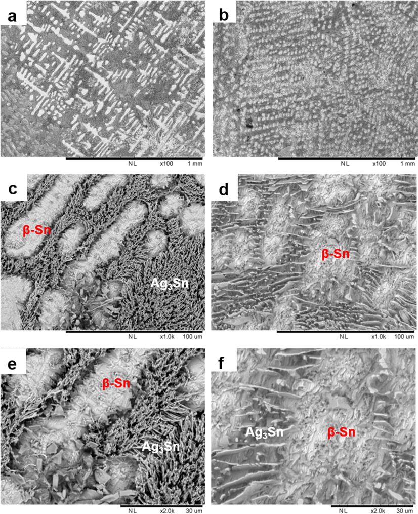
Microstructure at the solder bulk of (a, c, e) SAC305 and (b, d, f) SAC305/0.07GNP obtained by SEM at different magnifications.
It is widely reported that the addition of reinforcement materials to the solder composite will refine the grains of the matrix and IMCs (Tsao et al., 2012, Liu et al., 2016, Skwarek et al., 2020). In this case, the addition of graphene acted as a barrier to reduce the diffusion of Sn, Ag, and Cu in the solder during the reflow process. The inhibition of the movement of these elements prevents the growth of Ag3Sn and Cu6Sn5 IMC through Zener pinning effect (Kotadia et al., 2012, Mokhtari et al., 2012). Therefore, the grains of Ag3Sn in the composite solder obtained after reflowing would become finer when compared to the pure solder. Meanwhile, enhanced thermodynamic resistance of the IMC growth due to increased interfacial energy between IMC and graphene might contributed to the decreasing size of the IMCs (Liu et al., 2013). Besides that, refinement of phases due to the additions of graphene can also be directly related to heterogenous nucleation that took place (Greer and Quested, 2006). The additions of graphene allow solidification nucleation initiated on the graphene as foreign materials in the system. As a result, the undercooling needed for solidification process was reduced, which directly allows solidification to initiated on much smaller critical radius of the nucleus (Greer and Quested, 2006). This produced much smaller solidified grains as seen in this work, thus making it hard to observe the Cu6Sn5 grains in the solder using TM-SEM.
3.5.2 Cross-section
Selective electrochemical etching has successfully revealed a detailed microstructure of the pure SAC305 solder and SAC305/0.07GNP. The scallop shaped Cu6Sn5 is clearly observed in the SEM images (Fig. 5a). The Ag3Sn IMC is also seen near the interface area with a platelike shape. Besides, the presence of hexagonal Cu6Sn5 IMC is also clearly depicted in the SEM images.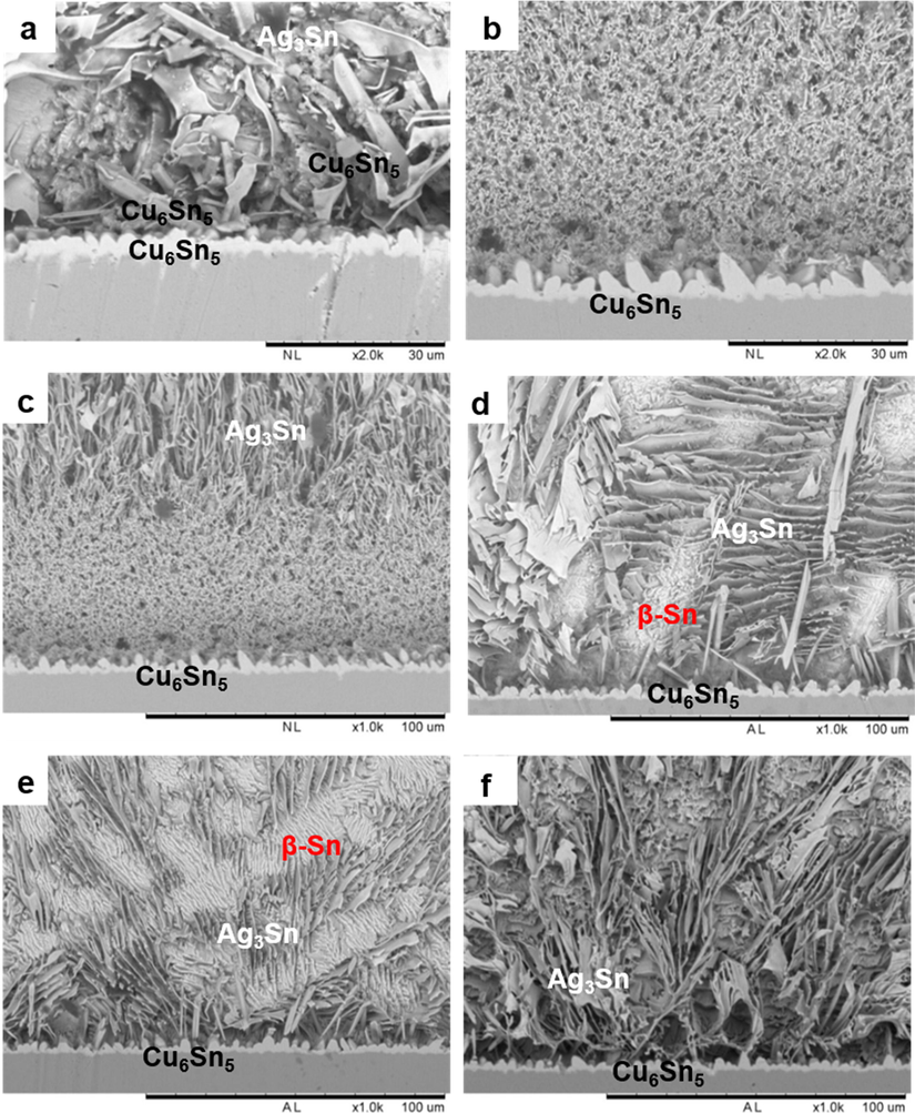
Cross sectional microstructure of (a) SAC305 solder and (b) SAC305/0.07GNP composite solder after etching at −350 mV potential bias; cross sectional microstructure of SAC305/0.07GNP after etching at (c) −350 mV, (d) −440 mV, (e) −480 mV for 240 s and (f) −480 mV for 480 s.
However, the platelike Ag3Sn and hexagonal Cu6Sn5 are not detected in the composite solder (Fig. 5b). It was hypothesized that the microstructure of composite solder near the solder/substrate interface was dissolved during selective electrochemical etching. The application of etching potential of −350 mV has exceeded the dissolution potential of IMC in the composite solder due to coupling effect with the nearby Cu substrate. Therefore, the IMCs in the composite solder dissolved during selective electrochemical etching.
Selective electrochemical etching was reconducted on the composite solder with a lower etching potential. The application of electric potential of −440 mV and −480 mV for 240 s has successfully etched the cross-section area of composite solder without damaging the microstructure (Fig. 5d-e). It is also observed that the increment of etching time at −480 mV potential from 240 s to 480 s produces more detailed images of the composite solder microstructure (Fig. 5f).
Based on the best microstructure image for composite solder obtained by electrochemical etching with −480 mV potential for 480 s, it was observed that the scallop shaped Cu6Sn5 does not undergo significant changes in its shape and size upon the addition of graphene (Fig. 5a, f). However, the Ag3Sn network near the interface is finer for the composite solder than the pure solder. It was also noticed that the hexagonal Cu6Sn5 is not present in the composite solder.
As discussed in the previous section, the refinement of Ag3Sn grain size for composite solder is attributed to the addition of graphene, which acts as a barrier to reduce the movement of the solder elements during the reflow process. The hexagonal Cu6Sn5 is not detected in the composite solder because the fraction of Cu in the solder is low and the movement of Cu is impeded by the presence of graphene in the solder.
3.5.3 Graphene location in composite solder
Although the microstructure analysis performed in the previous section showed the effect of graphene addition to the microstructure of SAC305, it was noted that the images of graphene nanoparticles are not captured in the microstructure. In this section, the microstructure analysis on cross-sectional images of SAC305/0.07GNP composite solder was further used to examine graphene location in the microstructure of the solder composite (Fig. 6a). Higher magnification clearly showed that graphene nanoparticles agglomerated in the solder/substrate interface (Fig. 6b-d).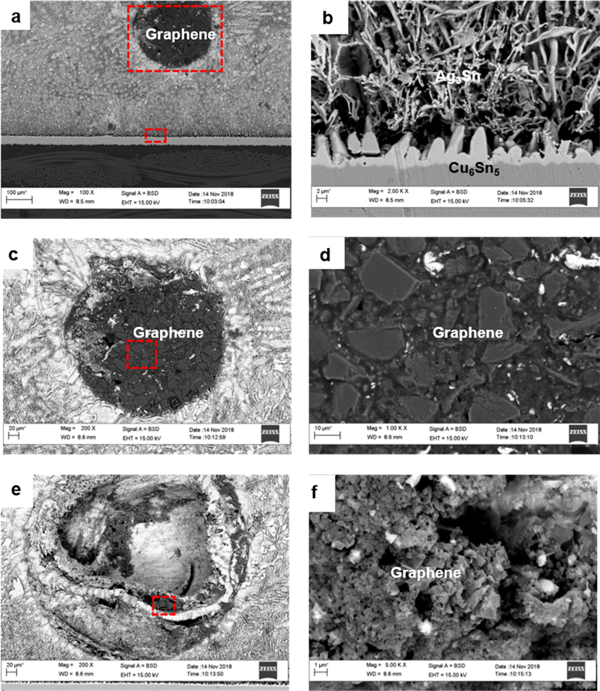
(a) Cross sectional FESEM images of SAC305/0.07GNP composite solder at area near solder/substrate interface; (b) higher magnification images of solder/substrate from (a); (c) magnified images of graphene agglomeration from (a); (d) magnified image of (c); (e) another graphene agglomeration at area along the solder/substrate interface; (f) magnified image from (e).
FESEM images captured at another area near the solder/substrate interface showed a round shaped void (Fig. 6e). It is believed that this void is also formed due to graphene agglomeration. However, the graphene agglomerates might fall off during preparation of the cross-sectional sample, thus leaving a void area. Higher magnification images of the void area also showed the presence of graphene (Fig. 6f).
Graphene agglomeration was also detected during FESEM observation at cross-sectional area near the solder surface (Fig. 7a-7d). However, the size of graphene agglomeration in this area is finer compared to the graphene agglomeration at area near the solder substrate interface. Higher magnification images also showed that the texture of graphene agglomerates at the area near the solder surface is looser compared to the one at the area near the solder/substrate interface.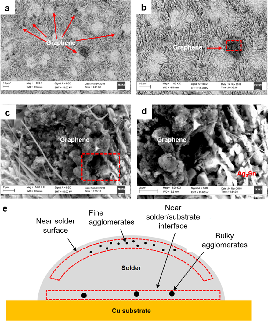
(a) FESEM images of graphene agglomeration at area near the solder surface; (b) magnified image of (a); (c) higher magnification images of the designated area in (b); (d) higher magnification images of designated area in (c), and (e) schematic of graphene agglomeration area in SAC305/0.07GNP composite solder.
Graphene agglomeration is normally attributed to the strong Van der Waals force, which attracts graphene particles to each other (Xu et al., 2016). The high surface area characteristic of graphene also enhances the attraction and promotes agglomeration. The agglomeration of carbon-based reinforcement is also a common phenomenon in composite solder. The addition of GNS would lead to pitting at the surface of composite solder (Liu et al., 2013). A similar type of pitting formation was also reported by other work (Xu et al., 2015).
However, this work found that the sizes and shapes of graphene agglomerates in the solder composite are different at different areas of the solder. At the area near the solder/substrate interface, graphene tends to form bulky round shaped agglomerates with a compact texture (Fig. 7e). Meanwhile, at the area near the solder surface, the graphene agglomerates are finer and slightly scattered. The differences in the size and shape of the graphene agglomerates could be related to the graphene movement during the reflow process.
3.6 Mechanism of graphene expulsion in SAC305/0.07GNP composite solder
The graphene movement and expulsion mechanism in SAC305/0.07GNP solder during reflow is proposed based on the experimental result obtained in previous sections (Fig. 8). In summary, the experimental results in this chapter give three information about graphene location inside and outside the solder bump after the reflow process;
-
Physical observation after reflows showed that graphene nanoparticles are spotted on top of the solder bump after reflow. This observation indicated that some portions of graphene nanoparticles are expelled from the solder during the reflow process.
-
Microstructure analysis on the cross-sectional area of the composite showed that large graphene agglomerates are found at the area slightly above the solder/substrate interface.
-
Microstructure analysis of composite solder also showed that fine graphene agglomerates reside in the solder near the solder surface.
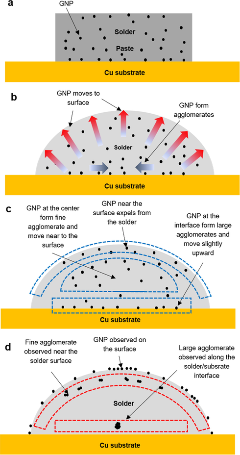
- Schematic for graphene movement and expulsion during the reflow process of SAC305/0.07GNP.
It is known that graphene nanoparticles are dispersed in the solder paste before the reflow process (Fig. 8a). However, the experimental observations listed above clearly signal that the graphene nanoparticles do not retain their position during the reflow process. The movement of graphene nanoparticles during reflow process could be attributed to two factors. First, the strong Van der Waals force between each graphene particle caused the particles to attract to each other, thus forming agglomerates (Luan et al., 2017). Second, graphene nanoparticles are flushed along with the flux during reflow process (Osorio et al., 2012). The buoyancy effect of the low-density graphene in liquid state solder might also contribute to the expulsion. It is believed that both types of movement occur simultaneously during reflow process (Fig. 8b).
The agglomeration and expulsion of all graphene nanoparticles in the solder occurs at the same rate. It is proposed that graphene nanoparticles residing near the solder surface are totally expelled from the solder (Fig. 8c-8d). However, graphene nanoparticles that reside in the centre of the solder bump are not expelled but form fine agglomerate at the area near the solder surface. Meanwhile, graphene nanoparticles residing at the solder/substrate interface form large agglomerates at the area slightly above the solder/substrate interface.
4 Conclusion
In this study, microstructural evaluation of Sn-3Ag-0.5Cu/0.07GNP composite solder was successfully done using selective electrochemical etching. The following conclusions were drawn from the study results:
-
Addition of 0.07 wt% of graphene does not alter the texture of SAC305 solder paste, while retaining the original phases for SAC305. However, significant refinement in microstructure of β-Sn and Ag3Sn was observed.
-
The study on electrochemical dissolution mechanism of SAC305 suggests that the dissolution of IMC will not happen unless all β-Sn are removed first from the solder. However, it is preferred to use a voltage value lower than −350 mV for electrochemical etching to avoid IMC dissolution during the process.
-
After electrochemical etching process, it was revealed that GNP in SAC305 existed in two forms of fine agglomeration on the surface of the solder, and large agglomeration at the solder/Cu substrate interface. The presence of large agglomeration of GNP acted as diffusion barrier that hindered the diffusion of Cu.
CRediT authorship contribution statement
Ibrahym Ahmad: Writing – original draft, Methodology, Investigation, Visualization, Project administration. Muhammad Firdaus Mohd Nazeri: Writing – review & editing, Investigation, Visualization, Validation. Nor Azmira Salleh: Writing – review & editing, Investigation, Visualization. Soorathep Kheawhom: Writing – review & editing, Conceptualization, Validation. Ahmet Mustafa Erer: Writing – review & editing, Validation. Adem Kurt: Writing – review & editing, Validation. Ahmad Azmin Mohamad: Supervision, Conceptualization, Writing – review & editing.
Acknowledgment
The authors appreciate the financial support provided by Tin Industry (Research and Development) Board Research Grant 2021 (304.PBAHAN.6050479.L114)
Declaration of Competing Interest
The authors declare that they have no known competing financial interests or personal relationships that could have appeared to influence the work reported in this paper.
Reference
- Investigation of anodic dissolution behaviour of intermetallic compound in Sn-3Ag-0.5 Cu solder alloy by cyclic voltammetry. Soldering Surf. Mount Technol.. 2019;31:211-220.
- [Google Scholar]
- Superior thermal conductivity of single-layer graphene. J. Nano Lett.. 2008;8:902-907.
- [Google Scholar]
- Effects of diamond nanoparticles reinforcement into lead-free Sn–3.0 Ag–0.5 Cu solder pastes on microstructure and mechanical properties after reflow soldering process. Mater. Des.. 2015;82:206-215.
- [Google Scholar]
- Retained ratio of reinforcement in SAC305 composite solder joints: effect of reinforcement type, processing and reflow cycle. Soldering Surf. Mount Technol.. 2016;28(3):159-166.
- [Google Scholar]
- Microstructures and properties of new Sn–Ag–Cu lead-free solder reinforced with Ni-coated graphene nanosheets. J. Alloys Compounds. 2016;656:500-509.
- [Google Scholar]
- Mechanically strong, electrically conductive, and biocompatible graphene paper. Adv. Mater.. 2008;20(18):3557-3561.
- [Google Scholar]
- Structural characterization and creep resistance of nano-silicon carbide reinforced Sn–1.0 Ag–0.5 Cu lead-free solder alloy. Mater. Des.. 2014;55:837-845.
- [Google Scholar]
- Optical properties of graphene. J. Phys.: Conf. Ser., IOP Publishing.. 2008;129:012004.
- [Google Scholar]
- Greer, A., T. Quested, 2006. Heterogeneous grain initiation in solidification. 86(24): 3665-3680.
- Interfacial reaction and shear strength of Ni-coated carbon nanotubes reinforced Sn–Ag–Cu solder joints during thermal cycling. Intermetallics. 2012;31:72-78.
- [Google Scholar]
- Sn–3.0 Ag–0.5 Cu nanocomposite solders reinforced by graphene nanosheets. J. Mater. Sci.: Mater. Electron.. 2016;27:6809-6815.
- [Google Scholar]
- Investigation of intermetallic compounds (IMCs) in electrochemically stripped solder joints with SEM. Microelectron. Reliability. 2012;52:1138-1142.
- [Google Scholar]
- Limitations of nanoparticle enhanced solder pastes for electronics assembly. In: 2012 12th IEEE International Conference on Nanotechnology (IEEE-NANO). IEEE; 2012. p. :1-5.
- [Google Scholar]
- Effect of graphene nanosheets reinforcement on the performance of SnAgCu lead-free solder. Mater. Sci. Eng.. 2013;562:25-32.
- [Google Scholar]
- Interfacial reaction of Sn-Ag-Cu lead-free solder alloy on Cu: A review. Adv. Mater. Sci. Eng.. 2013;2013 ID 123697
- [Google Scholar]
- Microstructure and mechanical properties of as-reflowed Sn58Bi composite solder pastes. J. Mater. Process. Technol.. 2016;238:290-296.
- [Google Scholar]
- Effect of intermetallic compounds on mechanical properties of copper joints ultrasonic-soldered with Sn-Zn alloy. J. Mater. Process. Technol.. 2017;248:123-129.
- [Google Scholar]
- Nanoparticle Enhanced Solders for Increased Solder Reliability. MRS Online Proc Library (OPL) 2012:1424.
- [Google Scholar]
- The effects of microstructure and Ag3Sn and Cu6Sn5 intermetallics on the electrochemical behavior of Sn-Ag and Sn-Cu solder alloys. Int. J. Electrochem. Sci.. 2012;7:6436-6452.
- [Google Scholar]
- Correlation between X-ray diffraction and Raman spectra of 16 commercial graphene–based materials and their resulting classification. Carbon. 2017;111:380-385.
- [Google Scholar]
- Effect of graphene nanoplatelets on wetting, microstructure, and tensile characteristics of Sn-3.0 Ag-0.5 Cu (SAC) alloy. Metall. Mater. Trans. A. 2016;47:494-503.
- [Google Scholar]
- Microstructure influence of SACX0307-TiO2 composite solder joints on thermal properties of power LED assemblies. Materials. 2020;13:1563.
- [Google Scholar]
- Safety and biocompatibility of graphene: A new generation nanomaterial for biomedical application. Int. J. Biol. Macromol.. 2016;86:546-555.
- [Google Scholar]
- Influence of TiO2 nanoparticles addition on the microstructural and mechanical properties of Sn0. 7Cu nano-composite solder. Mater. Sci. Eng.: A. 2012;545:194-200.
- [Google Scholar]
- Design and performance of Ag nanoparticle-modified graphene/SnAgCu lead-free solders. Mater. Sci. Eng.: A. 2016;667:87-96.
- [Google Scholar]
- Effects of graphene nanosheets on interfacial reaction of Sn–Ag–Cu solder joints. J. Alloys Compounds. 2015;650:475-481.
- [Google Scholar]
- Preparation of colloidal dispersions of graphene sheets in organic solvents by using ball milling. J. Nanomater.. 2010;2010 ID: 528235
- [Google Scholar]