

Translate this page into:
Investigating the preparation process of excellent Cu3VSe4 absorption layer prepared by amine-thiol system
⁎Corresponding author at: School of Physics and Electronic Information, Inner Mongolia Key Laboratory for Physics and Chemistry of Functional Materials, Inner Mongolia Normal University, 81 Zhaowuda Road, Huhhot, Inner Mongolia 010022, China. 20170020@imnu.edu (Yanchun Yang),
⁎⁎Corresponding author. cjzhu@imu.edu.cn (Chengjun Zhu)
-
Received: ,
Accepted: ,
This article was originally published by Elsevier and was migrated to Scientific Scholar after the change of Publisher.
Abstract
Cu3VSe4 material has become a new kind of photovoltaic absorber due to its optical bandgap matching light-absorbing, abundant elements in crust, and high light absorption coefficient. Here, we prepared Cu3VSe4 thin films by amine-thiol method and investigated the preparation process of excellent Cu3VSe4 absorption layer for the first time. The effects of various Cu/V ratios on the morphology, structure, and electrical properties of the films are studied. XRD and Raman results show that pure-phase Cu3VSe4 films are obtained with the Cu/V ratios lower than 2.9. SEM results simply adjusting the Cu/V ratio cannot obtain a compact selenized Cu3VSe4 thin films. The best crystallinity of thin film with 2.8 of Cu/V ratio is named as Cu2.8VSe4 and selected as the representative. Though optimizing the selenization conditions, a dense morphology and good electrical properties of the absorption layer can be prepared under 570 °C of the high-temperature process. Our findings can lay the favorable foundation for high-efficiency Cu3VSe4 devices.
Keywords
Cu3VSe4 thin films
Amine-thiol method
Cu/V ratio
Selenization conditions

1 Introduction
Because they possess the adjustable optical bandgaps and excellent stability, the copper-based thin film solar cells have been rapidly developed and have become an important option for renewable energy. Among these thin film solar cells, CdTe, Cu(In,Ga)Se2, and Cu2ZnSn(S,Se)4 materials are representative and have also made great progress (Kurley et al., 2017; Nakamura et al., 2019; Yang et al., 2024). However, the scarce In, Ga and Te elements, and the highly toxic Cd element, have become the restricting CdTe and Cu(In,Ga)Se2 developments (Wang et al., 2020). High harmful defects density is also main limitation of Cu2ZnSn(S,Se)4 solar cells. The new copper-based photovoltaic materials need to be developed. Recently, the ternary copper-based Cu3MCh4 (M = V, Nb, Ta; Ch = S, Se, Te) semiconductor materials have been reported, and they have been confirmed as p-type semiconductors (Kehoe et al., 2015). Cu3VS4 and Cu3VSe4 materials have the optical bandgap matching with sunlight and be regarded as the absorption layer of photovoltaic devices. At present, there are a few reports of Cu3VS4 thin film (Mantella et al., 2018; Wen et al., 2021;), but few reports of Cu3VSe4 thin film. Liu et al. fabricated Cu3VSe4 nanocrystal and Cu3VSe4-FTO thin films with p-type characteristic and photocurrent of ∼4 μA/cm2 (Liu et al., 2020). Afterward, they reported the preparation process and properties of Cu3VSe4 nanosheets (Liu et al., 2020). Wu et al. prepared Cu3VSe4 nanocrystal by one-pot reaction in oil phase (Wu et al., 2022). Nano-structural Cu3VSe4 synthesis needs usually the long-chain ligand which is not friendly to the optoelectronic devices. Therefore, for the future photovoltaic applications, the preparation process of Cu3VSe4 thin films need be studied.
With the advantages of controlling the elemental ratios accurately, low cost, and simplicity of large-area preparation, the precursor solution approach is a particularly ideal process for the development and manufacture of thin-film solar cells (Qin et al., 2022; Zhang et al., 2019). And the commonly used precursor solution systems include DMSO (Ki and Hillhouse, 2011; Gong et al., 2020; Xin et al., 2015), DMF (Liu et al., 2015; Luan et al., 2019; Collord and Hillhouse, 2016), amine-thiol (Fu et al., 2018; Tian et al., 2018), MOE (Zhao et al., 2021) etc., here, the amine-thiol system is used to prepare the thin films. It is well known that amine-thiol system can dissolve the elemental metal, metal oxide, metal salt, elemental S, elemental Se powders, and so on (Zhao et al., 2021; Fu et al., 2016; McCarthy et al., 2015). Yang et al. prepared the pure Cu2ZnSnSe4 thin film solar cells by amine-thiol system (Yang et al., 2016). Therefore, the amine-thiol system is very suitable for solution-processed Cu3VSe4 thin films. High performance solar cells often require the dense absorption layer with the pure phase, low density of harmful defects, and high crystallinity. Whether Cu3VSe4 thin films prepared by the amine-thiol system can be used as the absorption layer of solar cells or not, their preparation process needs to be studied and optimized.
In this study, based on the thiol-amine solution system, through tuning the Cu/V feeding ratio in the precursor solutions, Cu3VSe4 thin films with various Cu/V ratios could be prepared, and their properties were also investigated. The optimal crystallinity of thin film with 2.8 of Cu/V ratio was confirmed. Based on this finding, further investigation was conducted to explore the influence of selenization conditions on the properties of Cu3VSe4 thin films.
2 Experimental sections
2.1 Cu3VSe4 precursor solution preparation
Learned from our previous work of Cu2ZnSn(S,Se)4 thin films (Yang et al., 2015), Cu3VSe4 precursor solution was prepared as followed: 2 mL of thioglycolic acid and 3 mL of ethanolamine were placed in a 25 mL of conical flask and fully mixed under stirring on 70 °C hot plate. Next, 1 mmol C10H14O5V and 3 mmol C4H6CuO4·H2O were dissolved into this solution under stirring at 100 °C for 60 min until they were completely dissolved in this solution. After that, 300 mg Se powder was added under stirring for 30 min at 70 °C. The obtained viscous solution was cooled to room temperature. Finally, 7 mL of C3H8O2 was added under stirring for 30 min at 0 °C, forming the clean Cu3VSe4 precursor solution with 3.0 of Cu/V ratio. By adjusting the amount of C4H6CuO4·H2O, the precursor solutions with different Cu/V ratios were formed.
2.2 Cu3VSe4 thin films preparation
The Cu3VSe4 precursor solutions with various Cu/V ratios were spin-coated on the Mo-sputtered soda-lime glass with 3900 rpm for 40 s, which was annealed on 320 °C for 1.5 min. This step repeated five times to obtain the as-deposited Cu3VSe4 thin films with different Cu/V ratios. Finally, as-prepared Cu3VSe4 thin films were selenized by two-step selenization processes. These selenization processes consisted of the same low-temperature condition (400 °C,10 min) and the different high-temperature conditions (550 °C, 30 min; 560 °C, 30 min; 570 °C, 30 min; 580 °C, 30 min).
2.3 Characterization
The phase purity was achieved by X-ray diffraction (XRD) and Raman spectra. XRD pattern of thin films was measured on Empyrean powder, and Raman spectra was recorded on a HORIBA LabRAM ARAMIS. The micro-morphology was collected using scanning electron microscopy (SEM, Hitachi SU4800) and atomic force microscope (AFM, C-ypher,). The compositions of thin films were characterized by Energy dispersive spectrometry (EDS, built on the SEM). Average surface current was acquired using the conductive atomic force microscope (c-AFM) with a bias voltage of 2 V. Valence state was detected using the X-ray photoelectron spectroscopy (XPS) by a Thermo CIENTIFIC Nexsa.
3 Results and discussion
The absorption layer prepared by thiol-amine solution system usually involves two steps. Firstly, the as-deposited thin films are prepared by spin-coating precursor solution, and then the as-deposited thin films are selenized in high-temperature rapid thermal processing furnace to obtain absorption layer. Note that the extra Se needs be introduced in the selenization process, which is intended to provide the sufficient selenium vapor to promote the grain growth process and obtain a well-crystallized film. Here, the as-deposited Cu3VSe4 thin films prepared by thiol-amine solution system are nanostructured and porous, with a thickness of approximately 0.99 μm (Fig. S1 and 2). By adjusting the feed ratios of Cu and V sources, the Cu3VSe4 precursor solutions with different Cu/V ratios were prepared, and the corresponding as-deposited Cu3VSe4 thin films were also obtained by spin-coating these precursor solutions. Learned from Cu2ZnSn(S,Se)4 thin films’ experimental experiences, two-step selenization process is helpful for the crystallinity of the absorber, so all Cu3VSe4 thin films with various Cu/V ratios could be selenized by the same two-step selenization process (Yin et al., 2022; Ren et al., 2020; Mi et al., 2022). The Cu/V ratio in films is observed to increase proportionally with the increasing Cu/V ratio in precursor solution (Fig. 1a). Fig. 1(b) shows XRD patterns of the selenized Cu3VSe4 thin films with various Cu/V ratios. All films present the same diffraction peaks at 15.9°, 27.7°, 36.1°, 46.1°, and 54.7°, which can correspond to the (1 0 0), (1 1 1), (2 1 0), (2 2 0), and (3 1 1) planes, respectively, and exhibit the standard cubic structure. When the ratio of Cu/V is over 2.8, the diffraction peaks of Cu2S appear. In order to further validate the phase purity of Cu3VSe4 films, Raman spectra measurement can be used, as shown in Fig. S3. All samples have the vibration peaks at around 127, 149, 175, 210, 253, and 337 cm−1 which belong to the Cu3VSe4 phase, and no impure phase is observed, which is consistent with the reported literature (Zhai et al., 2023). Therefore, the pure phase of Cu3VSe4 films needs to control the Cu/V ratio is less than 2.9.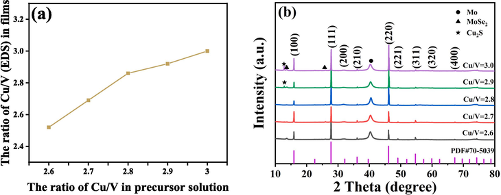
(a) Relationship Cu/V ratios in films with the feeding ratio of Cu/V in precursor solution and (b) XRD patterns of the selenized Cu3VSe4 films with various Cu/V ratios.
In order to investigate the morphology of Cu3VSe4 films with various Cu/V ratios, SEM measurement is carried out to elevate the morphology of all samples as shown in Fig. 2. When the feeding ratio of Cu/V is relatively small (∼2.6), the enlarged grains are dispersed on the surface of the selenized Cu3VSe4 thin films, resulting in a low coverage. As the feeding ratio of Cu/V increases, the coverage of the film increases and the film begins to become dense. The selenized Cu3VSe4 thin films present the best compactness until the Cu/V ratio is 2.8, and the impure phase (as circled in red) can appear with 3.0 of Cu/V ratio. The region circled in red can be observed to present a hexagonal phase which is consistent with the reported Cu2S phase (Sigman et al., 2003). Besides, the diffraction peaks of Cu2S phase can be detected in XRD patterns. Therefore, the region circled in red thought to be Cu2S phase. The presence of impure phase is fatal to high-quality absorption layers. The selenized Cu3VSe4 thin films with Cu/V ratio higher than 2.9 are not suitable as candidates for high-quality absorption layers. Meanwhile, the low coverage of the films with 2.6 of Cu/V ratio is also not considered further. So, the selenized Cu3VSe4 thin films with Cu/V ratio of 2.75 and 2.85 are supplemented. Fig. 3 and Fig. S4 show XRD patterns and SEM images of these selenized Cu3VSe4 thin films. All diffraction peaks are coincident with the above samples’ ones, and can belong to (1 0 0), (1 1 1), (2 1 0), (2 2 0), and (3 1 1) planes, respectively. Based on our experiment experience, (1 0 0) is dominant orientation in the Cu3VSe4 crystal growth, so the corresponding enlarged (1 0 0) peaks can be observed in Fig. 3b. The crystallinity of films can possess the optimal with 2.8 of Cu/V ratio, but the compactness of all films is still poor. And there appears to be a little peak shift, which is attributed to the enlarged grain. These conclusions indicate the Cu/V ratio has little impact on the compactness of selenized Cu3VSe4 films.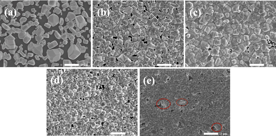
SEM images of Cu3VSe4 films with the various Cu/V ratios. (a) 2.6, (b) 2.7, (c) 2.8, (d) 2.9, (e) 3.0.
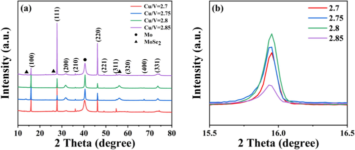
(a) XRD patterns of the selenized Cu3VSe4 thin films with various Cu/V ratios and (b) the corresponding enlarged (1 0 0) peaks.
The electrical properties of microscopic dense regions in above films are studied and depicted in Fig. 4. The chose scanning region is 3 × 3 μm2. The average surface roughness of the samples is calculated, as shown in Fig. S5. A decreased average surface roughness can be from 96.7 nm to 68.6 nm, with the increasing ratio of Cu/V, which should stem from the improved coverage of films. Afterwards, 2 V bias voltage is applied to observe the surface current distribution in the films. It can be seen that the sample with 2.8 of Cu/V ratio has the most and clearest current distribution, and its average current can reach 1.55nA, which indicates that it has the best carrier transport performance. All results show Cu3VSe4 thin films with 2.8 of Cu/V ratio are valuable for the absorption layers, and their properties are worth studying. And Cu3VSe4 thin films with 2.8 of Cu/V ratio are named as Cu2.8VSe4 thin films.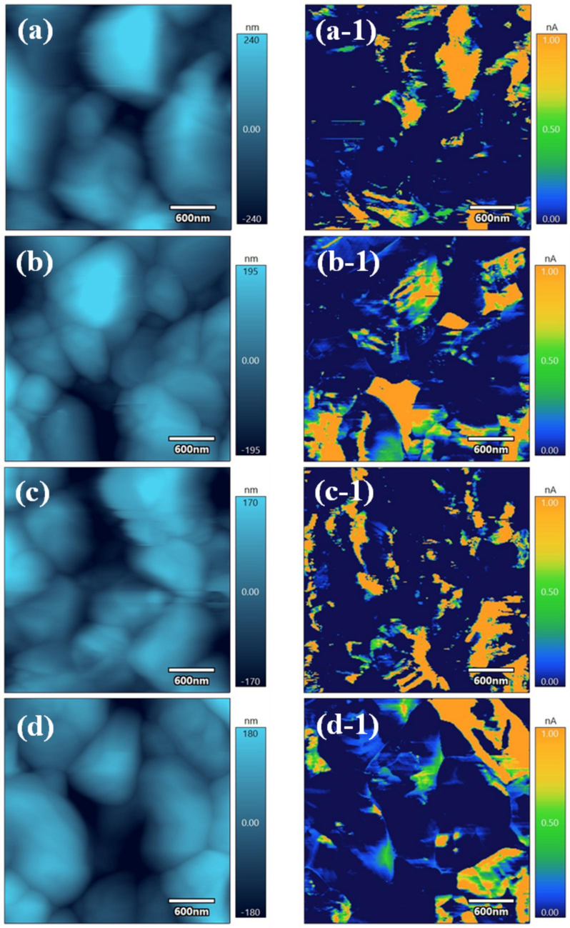
AFM and c-AFM images of the selenized Cu3VSe4 films with the various Cu/V ratios. (a, a-1) 2.7, (b, b-1) 2.75, (c, c-1) 2.8, (d, d-1) 2.85.
The primary factor for the outstanding absorption layer is a dense thin film, and the selenization process of the Cu2.8VSe4 thin films also needs to be further optimized. Here, our selenization process is the two-step selenization method, and its high-temperature process is known to be closely related to the compactness of the film. Therefore, we optimized the high-temperature selenization (HT) process of the Cu2.8VSe4 film. Based on our experiment experience (Ren et al., 2024), the optimal selenization time of Cu3V(S,Se)4 films is confirmed at 30 min, so the selenization time of the Cu2.8VSe4 film is also selected as 30 min. Fig. 5 shows SEM images of films with the different temperatures of HT process. As the temperature of HT process increases, the crystal size increases, the compactness of Cu2.8VSe4 films improves, and the large-grain layer thickens. Under the selenization condition of 570 °C, the film becomes completely dense, meeting the basic requirement of a high-quality absorption layer. And the corresponding XRD patterns (Fig. 6) are used to assess the phase purity and crystal structure of Cu2.8VSe4 film. Except for Mo peak, all peaks can be attributed to Cu3VSe4 phase, proving that all films are pure phases. The same peak positions demonstrate the temperature of HT process affects a little the crystal structure of Cu2.8VSe4 film, but has the significant impact on the crystallinity of Cu2.8VSe4 film. According to half-high width of diffraction patterns (Table S1), An increased average crystal size of Cu2.8VSe4 film is obtained with the increased selenization temperature, which is similar to that observed under SEM. And Cu2.8VSe4 film with the HT temperature of 570 °C is defined as the best sample. Besides, the valence states of main elements in the best sample are also studied, as shown in Fig. S6. The peak of Cu 2p appears at 932.7 and 952.5 eV, and the maximum split value is 19.8 eV (Mohammadnezhad et al., 2020; Zhang et al., 2020). The peak of V 2p is located at 513.9 eV and 521.6 eV, with the maximum split value of 7.7 eV (Liu et al., 2020). Se 3d peak is located at 54.1 eV and 55.2 eV, and the split value is 1.1 eV (Xue et al., 2021). These split values correspond to Cu+, V5+, and Se2-, respectively.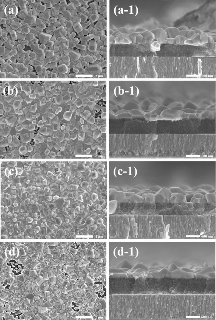
SEM images of Cu2.8VSe4 films with the different temperatures of HT process. (a, a-1) 550 °C, (b, b-1) 560 °C, (c, c-1) 570 °C, (d, d-1) 580 °C.
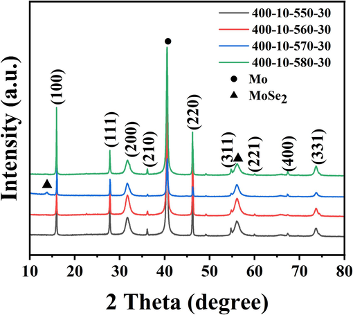
XRD patterns of Cu2.8VSe4 films with the different temperatures of HT process.
Fig. 7 shows the other properties (AFM, c-AFM images, absorption spectrum and Tauc curve) of the best sample. AFM and c-AFM images (Fig. 7a and b) show the best sample present the nice topography and low average surface roughness (∼51.516 nm), and the average surface current can be improved to 1.974nA. The absorption characteristic of the best film is assessed in Fig. 7c. There are three peaks located at around 435, 500, and 624 nm, respectively, which indicates the signature of the nanoscale sulvanites Cu3VSe4 phase. When converting wavelength in photo energy, these three absorption bands correspond to 3.17 eV, 2.20 eV and 1.83 eV which are in accordance with bandgap of VB-CB, VB-IB I, and VB-IB II, respectively (Oguchi et al., 1980; Bastola et al., 2018). This result shows the prepared Cu2.8VSe4 material possesses the intermediate bandgap. And there are two tuning points at 1.76 and 2.23 eV in the Tauc curve, which indicates further the intermediate band of Cu2.8VSe4 sample. These results demonstrate Cu2.8VSe4 film with the HT temperature of 570 °C can be regarded as the absorption layer of photovoltaic devices.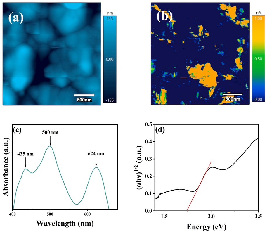
The other properties of the best sample. (a) AFM image, (b) c-AFM image, (c) absorption spectrum, (d) Tauc curve.
4 Conclusion
In summary, Cu3VSe4 thin films were prepared by thiol-amine solution system for the first time, and the preparation process of the excellent Cu3VSe4 absorption layer was also studied. The feeding ratio of Cu/V need be controlled below 2.9 to obtain pure phase Cu3VSe4 films, but it has little effect on the compactness of the films. And the reasonable properties of films with 2.8 of Cu/V ratio (named as Cu2.8VSe4 film) can present the potential candidate of absorption layer. Based on Cu2.8VSe4 film, by further optimizing the selenization process of the films, the pure phase, compact, and benign electrical properties of Cu2.8VSe4 absorption layer films can be achieved under 570 °C of the high-temperature process, which is suitable for the photovoltaic devices.
CRediT authorship contribution statement
Yanqing Liu: Conceptualization, Data curation, Formal analysis, Investigation, Methodology, Validation, Writing – original draft. Yanchun Yang: Funding acquisition, Project administration, Resources, Supervision, Writing – review & editing. Junting Ren: Investigation, Visualization. Guonan Cui: Resources, Visualization. Xin Zhao: Visualization. Rui Wang: Investigation, Visualization. Lulu Bai: Visualization. Chengjun Zhu: Funding acquisition, Supervision.
Acknowledgements
This work was supported by National Natural Science Foundation of China (Grant No. 62164010, 61804085, and 62064010), China Postdoctoral Science Foundation (Grant No. 2019M653806XB).
Declaration of competing interest
The authors declare that they have no known competing financial interests or personal relationships that could have appeared to influence the work reported in this paper.
References
- Structural, optical, and hole transport properties of earth-abundant chalcopyrite (CuFeS2) nanocrystals. MRS Commun. 2018;8(3):970-978.
- [CrossRef] [Google Scholar]
- Germanium alloyed kesterite solar cells with low voltage deficits. Chem. Mater.. 2016;28(7):2067-2073.
- [CrossRef] [Google Scholar]
- Improving the performance of solution-processed Cu2ZnSn(S, Se)4 photovoltaic materials by Cd2+ substitution. Chem. Mater.. 2016;28(16):5821-5828.
- [CrossRef] [Google Scholar]
- Tuning the Se content in Cu2ZnSn(S, Se)4 absorber to achieve 9.7 % solar cell efficiency from a thiol/amine-based solution process. ACS Appl. Energy Mater.. 2018;1(2):594-601.
- [CrossRef] [Google Scholar]
- Sn4+ precursor enables 12.4 % efficient kesterite solar cell from DMSO solution with open circuit voltage deficit below 0.30 V. Sci. China Mater.. 2020;64:52-60.
- [CrossRef] [Google Scholar]
- Kehoe, A.B., Scanlon, D.O., Watson, G.W., 2015. The electronic structure of sulvanite structured semiconductors Cu3MCh4 (M= V, Nb, Ta; Ch= S, Se, Te): prospects for optoelectronic applications. J. Mater. Chem. C 3, 12236-12244. https://doi.org/10.1039/C5TC02760H.
- Earth-abundant element photovoltaics directly from soluble precursors with high yield using a non-toxic solvent. Adv. Energy Mater.. 2011;1(5):732-735.
- [CrossRef] [Google Scholar]
- Transparent Ohmic contacts for solution-processed, Ultrathin CdTe. ACS Energy Lett.. 2017;2 (1) https://doi.or-g/10.1021/acsenergylett.6b00587
- [Google Scholar]
- Liu, M., Lai, C.Y., Selopal, G. S., Radu, D.R., 2020a. Synthesis and optoelectronic properties of Cu3VSe4 nanocrystals. PLoS One 15 (5), e0232184. https://doi.org-/10.1371/journal.pone.0232184.
- Cascade synthesis and optoelectronic applications of intermediate bandgap Cu3VSe4 nanosheets. Sci. Rep.. 2020;10(1):21679.
- [CrossRef] [Google Scholar]
- Kesterite Cu2ZnSnS4 thin film solar cells by a facile DMF-based solution coating process. J. Mater. Chem. C. 2015;3(41):10783-10792.
- [CrossRef] [Google Scholar]
- Influencing mechanism of cationic ratios on efficiency of Cu2ZnSn(S, Se)4 solar cells fabricated with DMF-based solution approach. Sol. Energy Mater Sol. Cells. 2019;195:55-62.
- [CrossRef] [Google Scholar]
- Synthesis and size-dependent optical properties of intermediate band gap Cu3VS4 nanocrystals. Chem. Mater.. 2018;31(2):532-540.
- [CrossRef] [Google Scholar]
- McCarthy, C.L., Webber, D.H., Schueller, E.C., Brutchey, R.L., 2015. Solution‐Phase conversion of bulk metal oxides to metal chalcogenides using a simple Thiol-Amine solvent mixture. Angew. Chem. Int. Ed. 54 (29), 8378-8381. https://doi.or- g/10.1002/ange.201503353.
- Exploring the optimal two-step selenization process to enhance the performance of ionic liquid solution based Cu2ZnSn(S, Se)4 thin film solar cells. J. Alloys Compd.. 2022;909:164740 https://doi.or-g/10.1016/j.jallcom.2022.164740
- [Google Scholar]
- Synthesis of highly efficient Cu2ZnSnSxSe4-x(CZTSSe) nanosheet electrocatalyst for dye-sensitized solar cells. Electrochim. Acta. 2020;340:135954
- [CrossRef] [Google Scholar]
- Cd-Free Cu(In, Ga)(Se, S)2 thin-film solar cell with record efficiency of 23.35 %. IEEE J. Photovolt.. 2019;9(6):1863-1867.
- [CrossRef] [Google Scholar]
- Optical reflectivity spectrum of a CuFeS2 single crystal. J. Phys. Soc. Jpn.. 1980;48(1):123-128.
- [CrossRef] [Google Scholar]
- Above 10 % efficient electrodeposited Cu2ZnSn(S, Se)4 solar cell achieved by modifying precursor. Sol. Energy Mater Sol. Cells. 2022;242:111781
- [CrossRef] [Google Scholar]
- Solution-processed Cu3V(S, Se)4 absorbers for thin films solar cells. Ceram. Int. 2024
- [CrossRef] [Google Scholar]
- CZTSSe solar cell with an efficiency of 10.19 % based on absorbers with homogeneous composition and structure using a novel two-step annealing process. Sol. Energy. 2020;207:651-658.
- [CrossRef] [Google Scholar]
- Solventless synthesis of monodisperse Cu2S nanorods, nanodisks, and nanoplatelets. J. Am. Chem. Soc.. 2003;125(51):16050-16057.
- [CrossRef] [Google Scholar]
- Green atmospheric aqueous solution deposition for high performance Cu2ZnSn(S, Se)4 thin film solar Cells. Sol. RRL. 2018;2(12):1800233.
- [CrossRef] [Google Scholar]
- Promising Cd-free double buffer layer in CZTSSe thin film solar cells. Sci. China Mater.. 2020;64:288-295.
- [CrossRef] [Google Scholar]
- Thermoelectric properties of p-Type Cu3VSe4 with high seebeck coefficients. J. Alloys Compd.. 2021;879:160387
- [CrossRef] [Google Scholar]
- Cu-V bimetallic selenide with synergistic effect for high-rate and long-life sodium storage. J. Mater. Res.. 2022;37:3308-3317.
- [CrossRef] [Google Scholar]
- Lithium-doping inverts the nanoscale electric field at the grain boundaries in Cu2ZnSn(S, Se)4 and increases photovoltaic efficiency. Phys. Chem. Chem. Phys.. 2015;17(37):23859.
- [CrossRef] [Google Scholar]
- Electrochemical Mg2+ displacement driven reversible copper extrusion/intrusion reactions for high-rate rechargeable magnesium batteries. Adv. Funct. Mater.. 2021;31(10):2009394.
- [CrossRef] [Google Scholar]
- The multiple roles of Na ions in highly efficient CZTSSe solar cells. Small 20242307807
- [CrossRef] [Google Scholar]
- Solution-processed highly efficient Cu2ZnSnSe4 thin film solar cells by dissolution of elemental Cu, Zn, Sn, and Se powders. ACS Appl. Mater. Interfaces. 2015;7(1):460-464.
- [CrossRef] [Google Scholar]
- A general water-based precursor solution approach to deposit earth abundant Cu2ZnSn(S, Se)4 thin film solar cells. J. Power Sources. 2016;313:15-20.
- [CrossRef] [Google Scholar]
- A high-efficiency (12.5 %) kesterite solar cell realized by crystallization growth kinetics control over aqueous solution based Cu2ZnSn(S, Se)4. J. Mater. Chem. A. 2022;10:779-788.
- [CrossRef] [Google Scholar]
- Flexible optical limiters based on Cu3VSe4 nanocrystals. Nanoscale. 2023;15(25):10606-10613.
- [CrossRef] [Google Scholar]
- Fabrication of Cu2ZnSnS4 (CZTS) nanoparticle inks for growth of CZTS films for solar cells. Nanomaterials. 2019;9(3):336.
- [CrossRef] [Google Scholar]
- Simple one-pot synthesis of Cu4SnS4 nanoplates and temperature-induced phase transformation mechanism. CrystEngComm. 2020;22:1220-1229.
- [CrossRef] [Google Scholar]
- Ambient air-processed Cu2ZnSn(S, Se)4 solar cells with over 12 % efficiency. Sci. Bull.. 2021;66(9):880-883.
- [CrossRef] [Google Scholar]
- Local Cu component engineering to achieve continuous carrier transport for enhanced kesterite solar cells. ACS Appl. Mater. Interfaces. 2021;13(1):795-805.
- [CrossRef] [Google Scholar]
Appendix A
Supplementary data
XRD pattern, SEM surface and cross-sectional images of as-deposited Cu3VSe4 thin films. Raman spectra of the selenized Cu3VSe4 films with the various Cu/V ratios. Top view and cross-sectional SEM images of the selenized Cu3VSe4 films with the various Cu/V ratios. The average surface roughness of the Cu3VSe4 with the various Cu/V ratios. Half-high width of diffraction patterns of films with the different HT temperature. XPS spectra of the best sample. Supplementary data to this article can be found online at https://doi.org/10.1016/j.arabjc.2024.105839.
Appendix A
Supplementary data
The following are the Supplementary data to this article:Supplementary Data 1
Supplementary Data 1