

Translate this page into:
XRD and AFM studies of ZnS thin films produced by electrodeposition method
*Corresponding author soonminho@yahoo.com (Anuar Kassim)
-
Received: ,
Accepted: ,
This article was originally published by Elsevier and was migrated to Scientific Scholar after the change of Publisher.
Available online 15 June 2010
Abstract
The structure and morphology of ZnS thin films were investigated. ZnS thin films have been grown on an indium tin oxide glass substrate by electrodeposition method using zinc chloride and sodium thiosulfate solutions at room temperature. The X-ray diffraction patterns confirm the presence of ZnS thin films. From the AFM images, grain size decreases as the cathodic potential becomes more negative (from −1.1 to −1.3 V) at various deposition periods. Comparison between all the samples reveals that the intensity of the peaks increased, indicating better crystalline phase for the films deposited at −1.1 V. These films show homogeneous and uniform distribution according to AFM images. On the other hand, XRD analysis shows that the number of ZnS peaks increased as deposition time was increased from 15 to 30 min at −1.1 V. The AFM images show thicker films to be formed at −1.1 V indicating more favourable condition for the formation of ZnS thin films.
Keywords
Electrodeposition
Zinc sulphide
Complexing agent
Thin film

1 Introduction
The synthesis of binary metal chalcogenides in a crystalline form has been a rapidly growing area of research due to their important physical and chemical properties. Zinc sulphide is an important II–VI semiconductor with a wide band gap which is suitable for applications in solar cells, solar selective decorative coatings, UV light emitting diode, photocatalysis and phosphors in flat panel displays. ZnS thin films are non-toxic to human body, very cheap and abundant.
A variety of techniques such as SILAR (Ates et al., 2007), electrodeposition (Huang et al., 2008), chemical bath deposition (Zhou et al., 2009), spray pyrolysis (Yazici et al., 2003) and vacuum evaporation (Kumar et al., 2006) have been used for deposition of ZnS thin films. Among various other methods, the electrodeposition method is found to be a cheap and simple way to deposit large area polycrystalline metal chalcogenide thin films. The preparations of various thin films using electrodeposition method such as CdTe (Hernandez et al., 2001), SnS (Cheng et al., 2006), PbSe (Li et al., 2006), HgCdTe (Chauhan and Rajaram, 2008) and Cd1−xFexS (Deshmukh et al., 2005) have reported by several authors.
The use of complexing agent is very common in the preparation of thin films. The presence of complexing agent in an aqueous solution is found to improve the lifetime of the deposition bath as well as the adhesion of the deposited films on the indium tin oxide glass substrates. Many researchers use various complexing agents such as ammonia (Gaewdang and Gaewdang, 2005), triethanolamine (Zainal et al., 2005), disodium ethylene diamine tetra-acetate (Anuar et al., 2010), nitrilotriacetic acid (Khallaf et al., 2008) and tartaric acid (Hankare et al., 2003) during deposition of thin films.
The present studies are focused on the deposition of crystalline cubic ZnS thin films using an electrodeposition method. Here, we report for the first time the electrodeposition of ZnS thin films from an aqueous solution using zinc sulphate, sodium thiosulfate and triethanolamine solutions at room temperature. In order to get good quality ZnS thin films, the preparative parameters such as deposition time (15, 30 and 60 min) and deposition potential (−1.0, −1.1 and −1.3 versus SCE) were optimized. The deposited thin films were characterized by X-ray diffraction and atomic force microscopy for their structural and surface morphological characteristics, respectively.
2 Experimental
2.1 Preparation of thin films
All the chemicals used for the deposition were analytical grade reagents and all the solutions were prepared in deionised water (Alpha-Q Millipore). The zinc sulphide thin films were prepared from an acidic bath using aqueous solutions of zinc chloride (0.01 M) and sodium thiosulfate (0.05 M) acted as a source of Zn2+ and S2− ions, respectively. The concentrated triethanolamine was used as complexing agent to chelate with Zn2+ to obtain Zn-EDTA complex solution.
The EG&G Princeton Applied Research potentiostat driven by a software model 270 Electrochemical Analysis System was used for the zinc sulphide electrodeposition in a three-electrode cell. The cell consisted of indium doped tin oxide (ITO) glass substrate as working electrode, platinum wire as a counter electrode and a saturated calomel electrode (SCE) as reference electrode, separately. Before deposition, the glass substrate was degreased with ethanol for 10 min. Then, ultrasonically cleaned with distilled water for another 10 min and dried in desiccator.
Purified nitrogen was flowed into the deposition bath for few minutes to create oxygen free environment. The thin films were grown at pH of the solution that is 3. The pH was adjusted by using hydrochloric acid. The zinc sulphide thin films were prepared at various deposition periods (15, 30 and 60 min) and deposition potentials (−1.0, −1.1 and −1.3 V versus SCE) at room temperature. After the deposition, the thin films were washed with distilled water and kept for analysis.
2.2 Characterization of thin films
The structure of the film was monitored by X-ray diffraction (XRD) with a Philips PM 11730 diffractometer equipped with a Cu Kα (λ = 0.15418 nm) radiation source. Data were collected by step scanning from 20° to 60° with a step size of 0.05° (2θ). The surface morphology, thickness and roughness were examined by recording atomic force microscopy images with a Q-Scope 250 in contact mode with a commercial Si3N4 cantilever. Values of root mean square (RMS) roughness were calculated from the height values in the atomic force microscopy images using the commercial software.
3 Results and discussion
Fig. 1 shows the X-ray diffraction (XRD) patterns of zinc sulphide thin films deposited at various cathodic potentials at −1.0, −1.1 and −1.3 V versus SCE for 15 min. Aside from the diffraction peaks of the indium tin oxide (Nadaud et al., 1998) (reference code: 01-089-4597) substrate, those assigned to cubic of ZnS peaks are only seen in all the XRD patterns. All the diffraction peaks are identified as belonging to two groups. The peaks marked with solid diamonds are associated with reflections of the cubic structure of ZnS and those marked with open diamonds can be ascribed to the orthorhombic structure of indium tin oxide.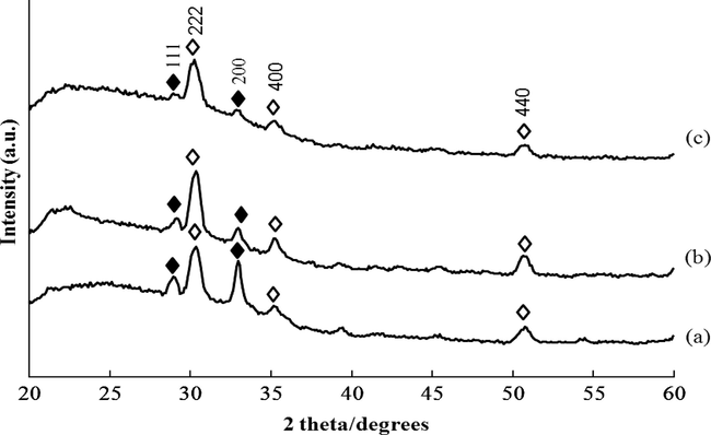
X-ray diffraction patterns of ZnS thin films deposited at different deposition potentials for 15 min (a) −1.0 V, (b) −1.1 V, and (c) −1.3 V (♦: ZnS; ⋄: In1.875O3Sn0.125).
The diffraction peaks from (1 1 1) and (2 0 0) corresponding to ZnS were observed. These peaks were identified by comparing the d-spacing values obtained from the XRD patterns with JCPDS (reference code: 00-065-0309) data for ZnS (Dubrovin et al., 1983). The lattice parameters of the cubic structure are equal to a = b = c = 5.4 Å. As the cathodic potential decreases, the intensity of the diffraction peaks increases, indicating the growth of the ZnS grains. At more negative potential (−1.3 V), the diffraction peaks of ZnS show weaker due to the thickness of ZnS films which became thinner. This was confirmed from AFM analysis.
Fig. 2 presents the atomic force microscopy (AFM) images of zinc sulphide thin films (20 × 20 μm) deposited at various cathodic potentials at −1.0, −1.1 and −1.3 V versus SCE for 15 min. The AFM images show that an increase in number of grains is found on the film surface along the negative shift of the deposition potential (from −1.0 to −1.3 V) which indicate that the grain size becomes progressively smaller. The grain size of ZnS films deposited at −1.0, −1.1 and −1.3 V are 1–1.5, 1.2 and 0.75–1 μm, respectively.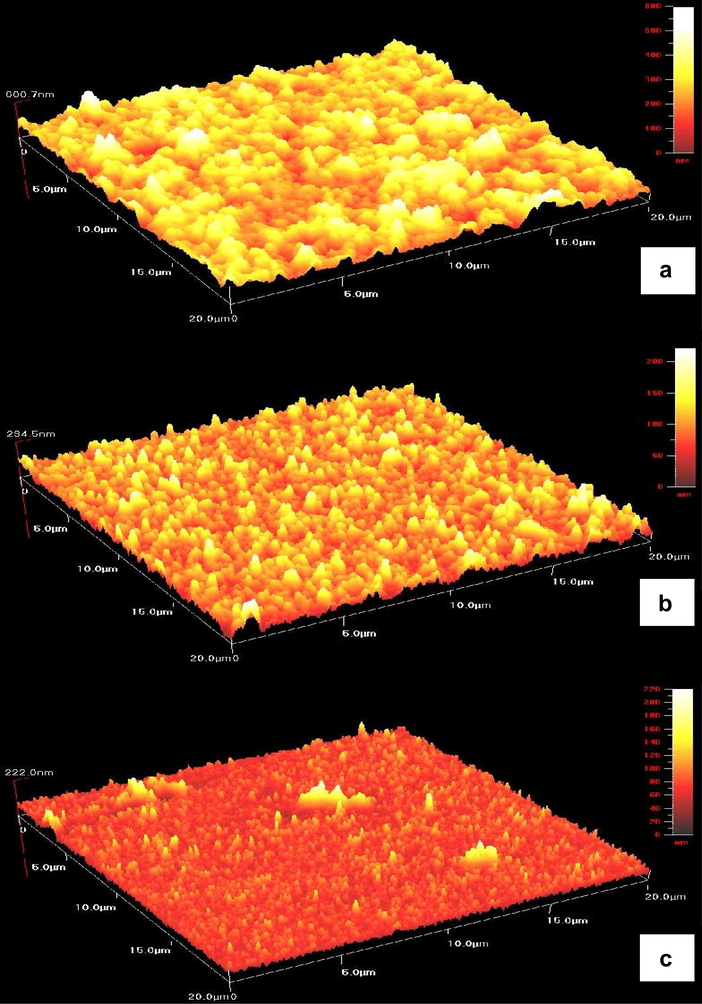
Atomic force microscopy images of ZnS thin films deposited at different deposition potentials for 15 min (a) −1.0 V, (b) −1.1 V, and (c) −1.3 V.
The grain size of thin films was determined from AFM images were carried out by many researchers (Murakami et al., 2007; Cheng et al., 2008; Datta et al., 2006). It is well known that AFM is one of effective ways for the surface analysis due to its high resolution and powerful analysis software. In our case, the grain size estimated directly from AFM images but not using the Scherrer equation. This could be explained by an agglomerate of many small grains in our samples. It can be seen that at lower cathodic potential (−1.0 V), the growth of thin films was found to be irregular.
This observation suggests an incomplete nucleation step with irregular growth rate of the grains. As a result, the films consist of larger and smaller grain size. However, the uniform grain size could be observed for the films prepared at higher cathodic potential (−1.1 V). The grains were packed very closely and showed a granular morphology.
The root mean square (RMS) roughness and thickness of the thin films were investigated using AFM images. Root mean square roughness is defined as the standard deviation of the surface height profile from the average height, is the most commonly reported measurement of surface roughness (Jiang et al., 2005). The three-dimensional AFM image shows that larger surface roughness (71 nm) and thicker films (601 nm) was observed for the films deposited at −1.0 V (Table 1). The surface roughness of the film is unavoidable since grains were grown with different sizes and spherical in shapes.
Film thickness (nm)
Root mean square roughness (nm)
Deposition potential (versus SCE) (V)
601
71
−1.0
235
25
−1.1
222
16
−1.3
Fig. 3 shows the X-ray diffraction patterns of zinc sulphide thin films deposited at various cathodic potentials at −1.0, −1.1 and −1.3 V versus SCE for 30 min. During deposition, the films prepared at a potential of −1.0 V show the presence of three major peaks corresponding to (1 1 1), (2 0 0) and (2 2 0) planes of ZnS. At higher cathodic potential (−1.1 V), an additional ZnS peak (3 1 1) was obtained as shown in Fig. 3b. As the cathodic potential increases further (−1.3 V), the disappearance of two diffraction peaks from (2 0 0) and (3 1 1) corresponding to ZnS was detected. Based on the XRD patterns, all the peaks can be indexed to cubic phase of ZnS and no impurity phase is detected.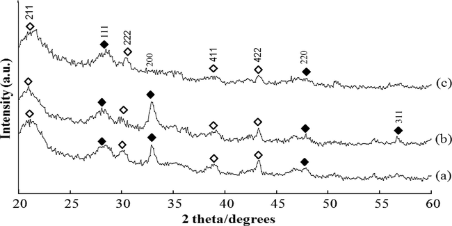
X-ray diffraction patterns of ZnS thin films deposited at different deposition potentials for 30 min (a) −1.0 V, (b) −1.1 V, and (c) −1.3 V (♦: ZnS; ⋄: In1.875O3Sn0.125).
On the other hand, the diffraction peaks in the XRD pattern are very sharp with the high intensity (Fig. 3b) indicating the significant increase in grain size. In contrast, the broadening of these diffraction peaks (Fig. 3a and c) indicates that the samples are small grain size. As the deposition potential was increased up to −1.1 V, the intensity of the peak corresponding to (2 0 0) plane increased. The (2 0 0) plane seems dominant at this stage of experiment. Similar (2 0 0) plane dominance was also reported by Zhu et al. (in press) for ZnS films prepared by cathodic electrodeposition technique. Therefore, the deposition potential plays an important role in the structure of ZnS thin films.
Atomic force microscopy (AFM) is a convenient technique to study the morphology of thin films. Fig. 4 presents the AFM images of zinc sulphide thin films (20 × 20 μm) deposited at various cathodic potentials at −1.0, −1.1 and −1.3 V versus SCE for 30 min. Initially, the grain size increased (0.5–1 μm to 2 μm) with the increase of cathodic potential from −1.0 to −1.1 V. It can be observed that the films are uniform, well defined, spherical and cover the substrate well.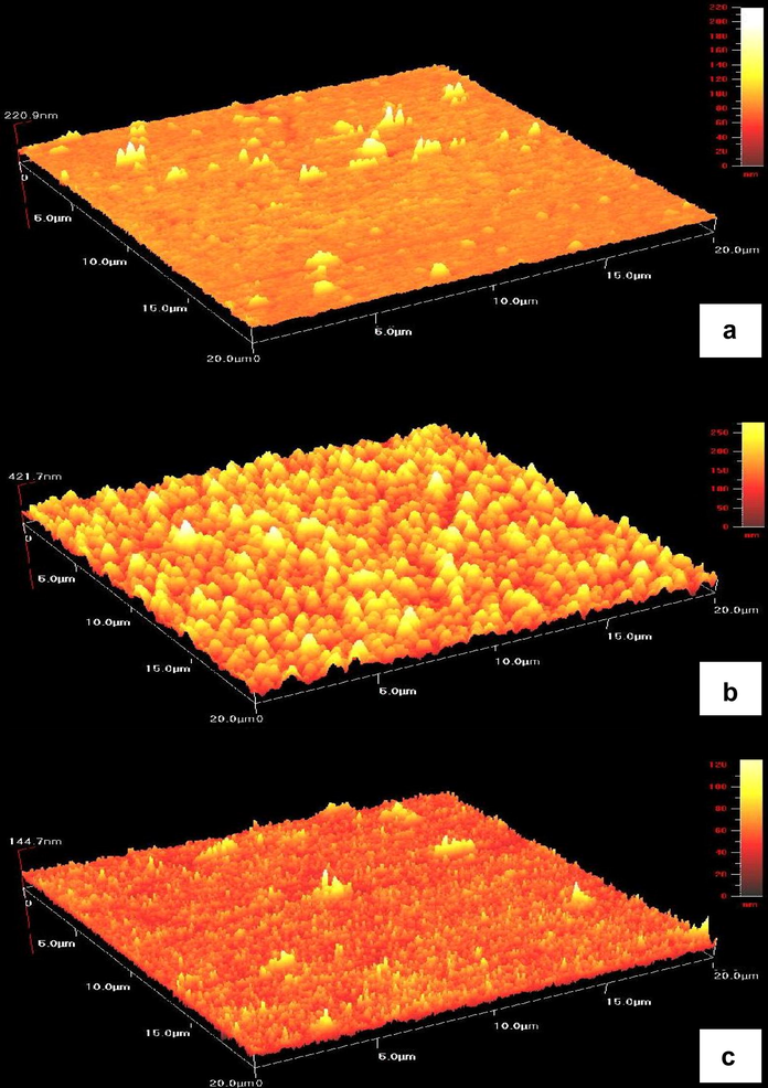
Atomic force microscopy images of ZnS thin films deposited at different deposition potentials for 30 min (a) −1.0 V, (b) −1.1 V, and (c) −1.3 V.
The spherical grains were also reported for ZnS thin films obtained by solution growth technique (Sadekar et al., 2008) and chemical bath deposition method (Nasr et al., 2006). The larger grain size of thin films may provide more surface area for liquid electrolyte/electrode junction photoelectrochemical (PEC) devices (Mahalingam et al., 2006). As deposition potential was moved more negative than −1.1 V, the grain size (0.3–0.6 μm) reduced at a potential of −1.3 V. Therefore, the deposition potential has a great influence on the grain size of the thin films.
From the AFM measurements, we obtained the root mean square (RMS) roughness and film thickness values (Table 2). In Fig. 4, at the right side of the images, an intensity strip is shown, which indicates the depth and height along the z-axis. It is clear that the thickness of the films increased as the deposition potential was increased up to −1.1 V.
Film thickness (nm)
Root mean square roughness (nm)
Deposition potential (versus SCE) (V)
221
8
−1.0
422
47
−1.1
145
9
−1.3
However, the thickness of films prepared at −1.3 V appears to be much thinner. On the other hand, the largest rough surface roughness (47 nm) of the films formed at −1.1 V was observed. We assume that grain growth and larger grains may be formed at this potential, resulting in higher RMS roughness.
Fig. 5 presents the X-ray diffraction patterns of zinc sulphide thin films deposited at various cathodic potentials at −1.0, −1.1 and −1.3 V versus SCE for 60 min. The major peaks shown by all samples correspond to reflections from (1 1 1) and (2 0 0) planes of cubic phase of ZnS. At lower cathodic deposition potentials (−1.0 and −1.1 V), both films exhibit an additional ZnS peaks corresponding to (2 2 0) and (3 1 1) planes.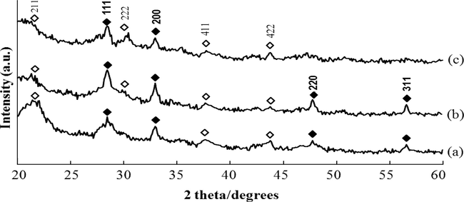
X-ray diffraction patterns of ZnS thin films deposited at different deposition potentials for 60 min (a) −1.0 V, (b) −1.1 V, and (c) −1.3 V (♦: ZnS; ⋄: In1.875O3Sn0.125).
Comparison between these thin films reveals that the intensity of the peaks increased, indicating better crystalline phase in the films which deposited at −1.1 V. However, at higher cathodic potential (−1.3 V), the number of peaks decreased to two indicating less favourable condition for the formation of ZnS thin films.
Fig. 6 presents the atomic force microscopy images of zinc sulphide thin films (20×20 μm) deposited at various cathodic potentials at −1.0, −1.1 and −1.3 V versus SCE for 60 min. At lower cathodic potential (−1.0 V), the ITO surface was totally covered by fine ZnS grains with diameter of 0.3 μm (Fig. 6a). However, the thicker films (film thickness of 216 nm) were obtained at this deposition potential (Table 3). This is due to the presence of a few larger grains in this sample. Fig. 6b shows the thin films deposited at a potential of −1.1 V. It is clearly seen that the grain size is relatively larger in size (0.7 μm) and comparatively rough (17 nm) than that of other samples.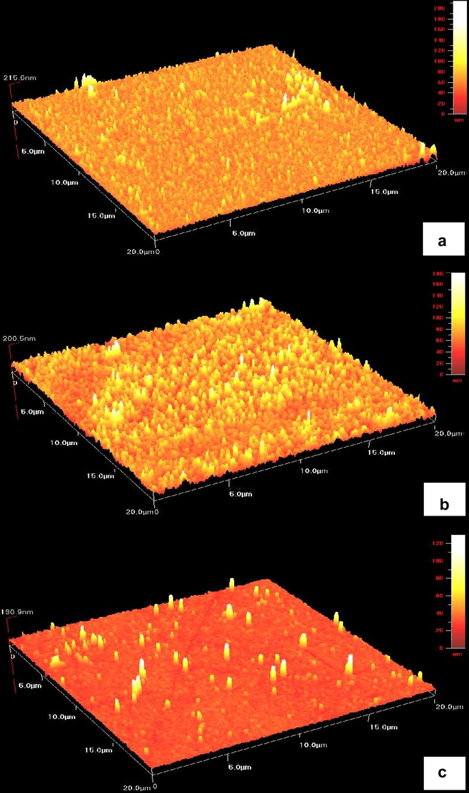
Atomic force microscopy images of ZnS thin films deposited at different deposition potentials for 60 min (a) −1.0 V, (b) −1.1 V, and (c) −1.3 V.
Film thickness (nm)
Root mean square roughness (nm)
Deposition potential (versus SCE) (V)
216
9
−1.0
201
17
−1.1
191
5
−1.3
These films are uniform, regular, homogeneous and without cracks. A very rough surface may be suitable for photoelectrochemical cell applications as it will capture more light. However, at higher cathodic potential (−1.3 V), it is seen that discontinuous and uneven distribution of grains on surface of ZnS thin films was obtained. According to AFM image, less visible films (191 nm) could be seen. This indicated that this deposition potential was not suitable for the electrodeposition of ZnS films.
4 Conclusions
ZnS thin films were prepared in an aqueous solution by using electrodeposition method. X-ray diffraction patterns indicate a cubic structure for the ZnS thin films. XRD patterns show that the intensity of the peaks increased, indicating better crystalline phase for the films deposited at −1.1 V for 30 min. AFM images indicate that regular, homogeneous surface and larger grain size was obtained under this conditions. From the above results, we can conclude that deposition the at −1.1 for 30 min is the best deposition parameters for the preparation of ZnS thin films under the current conditions.
Acknowledgement
The authors would like to thank the Department of Chemistry, Universiti Putra Malaysia for the provision of laboratory facilities and MOSTI for the National Science Fellowship (NSF).
References
- Asian J. Chem.. 2010;22:222-232.
- Mater. Sci. Semicond. Process.. 2007;10:281-286.
- Sol. Energy Mater. Sol. Cells. 2008;92:550-557.
- Opt. Mater.. 2006;29:439-444.
- Surf. Coat. Technol.. 2008;202:6070-6074.
- Appl. Surf. Sci.. 2006;253:2289-2295.
- Mater. Sci. Eng., B. 2005;122:206-210.
- Inorg. Mater.. 1983;19:1603-1608.
- Mater. Lett.. 2005;59:3577-3584.
- Mater. Chem. Phys.. 2003;82:505-508.
- Sol. Energy Mater. Sol. Cells. 2001;70:269-275.
- J. Synth. Cryst.. 2008;37:862-865.
- Thin Solid Films. 2005;417:76-85.
- Thin Solid Films. 2008;516:5967-5973.
- Indian J. Pure Appl. Phys.. 2006;44:690-693.
- J. Solid State Electrochem.. 2006;10:48-53.
- J. Mater. Sci.: Mater. Electron.. 2006;17:519-523.
- Thin Solid Films. 2007;515:8632-8636.
- J. Solid State Chem.. 1998;135:140-148.
- Mater. Chem. Phys.. 2006;96:84-89.
- J. Alloys Compd.. 2008;453:519-524.
- J. Lumin.. 2003;104:115-122.
- J. Mater. Sci. – Mater. Electron.. 2005;16:281-285.
- J. Environ. Sci.. 2009;21:S76-S79.
- Zhu, H., Huang, J.F., Wang, Y., Cao, L.Y., He, H.Y., Wu, J.P., in press. Surf. Eng. doi:10.1179/026708409x12490360426089.